CET1171 Lecture #6 - Circuit Buses and Motherboards
Materials: Working complete PCBlank DisketteStudent Diskette, "New Boot A Ver 2.0+" Working complete PCBlank DisketteStudent Diskette, "New Boot A Ver 2.0+"Objectives: The student should become familiar with: The general concept of a circuit bus,The major circuit buses of the PC,The role of the PC motherboard,The major types of motherboard,The basic components of the motherboard,Know all associated terminology including the meaning of acronyms.Competency: The student will understand the general concept of a digital circuit bus and learn the various circuit buses in the PC. The student will learn about the PC motherboard including its roles, form factors, and major components. |
Procedures
-
The computer itself is the CPU - Central Processing Unit, or microprocessor. Within this chip the actual execution of programs takes place in which data values are retrieved from RAM into the CPU and then mathematical operations are performed on these values and the results are then written back out to RAM.
-
While it might be possible to build a CPU that performs operations on one bit binary numbers it would still be impossible to fetch different data values and store them in RAM without the ability to address large numbers of RAM locations. This is where the buses come into play within the modern digital computers including the PC.
-
In lecture #4 the concepts of digital logical operations and logic gates were described. Within that lecture the internal functionality of a 3-bit demultiplexer was examined. This particular circuit, a digital demultiplexer, is the key to the function of one of the two major buses of the PC: the address bus. However, the basic definition of a bus must first be stated.
Definition: A bus is a set of parallel wires in which each wire carries one bit at a
 specific place value of a large binary number so that together they carry a large
binary number from one location in the computer to another. -
Let's first take a look at a simple illustration. On a wall there are three light switches marked "A", "B", and "C" Each switch as anyone would expect, can control one of the three recessed lights in the ceiling of the room. By flicking each one on and off, one can quickly tell which light is controlled by which switch. There is a one-to-one relationship between the switches and the lights that they control. In this case there are three lights and there are three switches; one for each light. Each switch controls only its light and has absolutely no effect on any other light. If another light is added, then another switch would have to be added to the wall panel. And if 100 new lights were installed, 100 new switches would have to be installed, one for each light. And if 1,000,000 new lights were installed then 1,000,000 new switches would also have to be added; one for each light.
-
However, what if some computer engineers were given the task of wiring the switches to the lights? While there are only three lights they might leave the current arrangement alone. However, once 100 or a 1,000,000 lights are added, the computer engineers would quickly move to using the switches in a new way. Instead of letting each one be wired through to each individual light and therefore needing one switch for each light, the engineers would group the switches together so that combinations of the states of the switches would select a particular light and then the state of one particular switch designated the "data" switch would then either turn the selected light on or off.
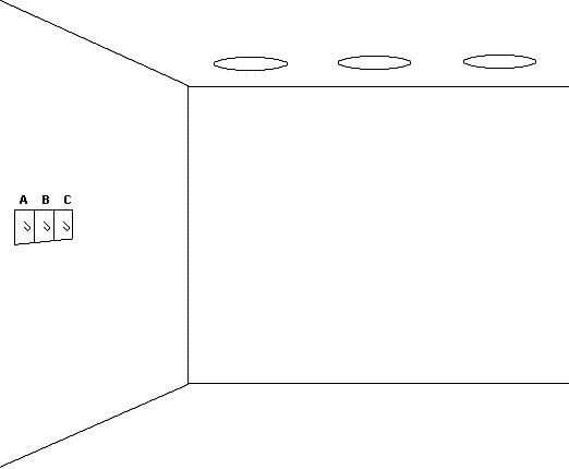
Three lights each controlled by a unique switch -
Using the demultiplexer circuit introduced in lecture #4, the three switches could be wired to this device. Upon setting a "data" switch ("D"), then the combination on the "selector" switches, a "send" switch ("S") would then be used to determine which light has been selected from the states of the selector switches, the data switch's state would then be read and the target light would then be set equal to it (i.e. on or off). This allows three switches with the additional Data switch and Send switch to control all possible combinations of the three switches:
 off-off-off = 000
 off-off-on = 001
 off-on-off = 010
 off-on-on = 011
 on-off-off = 100
 on-off-on = 101
 on-on-off = 110
 and on-on-on = 111
 Total of eight possible combinations.
-
So the set of switches can control eight lights. And the combinations of the switches are actually nothing more than the binary numbers from 000 to 111. Using 5 switches to control eight lights is certainly not impressive and probably not worth the trouble either. But eight switches with the D and the S switches can control 256 lights and 16 switches plus two could control 65,536. And just 32 switches plus the D and S switch could control 4,294,967,296 lights! This is the power of the bus. Instead of having to run an independent switch wire to each RAM memory cell which will work fine for a few hundred of them and allow the PC to hold programs the size of a programmable calculator, the system can use a group of wires which carry the numeric value of the desired RAM location as the place value binary number expressed as the combination of the states or voltages in these wires. This allows a set of 16 wires to select between 65,536 different memory locations and a set of 32 wires to select between over 4 billion RAM memory locations. This set of wires in the PC is called the address bus mentioned earlier and it is the key to the PC's immense computing power and the size and therefore intricacy and complexity of its programs and the data it manipulates as well.
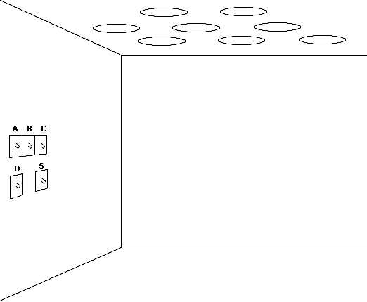
Eight lights controlled by the combination of the switches -
So in a simple three wire address bus the demultiplexer would be able to distinguish between eight particular RAM memory cells. And in a 16-wire address bus the demultiplexer can distinguish between 65,536 different RAM memory locations. There is a simple way to determine the number of numbers or addresses that a bus can distinguish between. Since each wire can carry either a "0" or a "1", then each wire carries two possible states. And there are a given number of wires resulting in the formula:
   stateswires = addresses (or number of distinct values)

   in binary systems the number of states is two (0 or 1) so:

   2wires = addresses (or number of distinct values)
-
So for a three wire binary address bus: binary means two states, so 23 = 8. And for a 16 wire binary bus: 216 = 65,536. And for a 32 wire address bus: 232 = 4,294,967,296. The actual addresses themselves in the case of the 3-wire bus which can address 8 distinct addresses are 000 to 111 or 0 to 7. So a 16-wire bus can address 65,536 distinct addresses which are 0000 0000 0000 0000 to 1111 1111 1111 1111 or 0 to 65,535. The lowest valid address is always zero on any of these binary buses. The highest actual address on the bus is given by the formula:
   stateswires - 1 = highest address (or distinct value)

   in binary systems the number of states is two (0 or 1) so:

   2wires - 1 = highest address (or distinct value)
-
The address bus of the PC runs from the CPU through the mounting socket or slot into the copper traces across the motherboard to the bus controller circuitry of the motherboard chipset and ultimately to the RAM expansion modules which contain some of the demultiplexer circuitry for converting the binary place value number that the CPU places on the address bus into the actual activation signal of the RAM memory location that is being addressed. The motherboard also handles some of the RAM address demultiplexing process as well allowing the RAM modules to be "relocatable" If the actual addresses were completely hard wired into each memory cell on the module then a particular module would have to be inserted into the first RAM expansion slot and the next one would have to be inserted into the next slot and so on. This partial demultiplexing or address translation is part of the strength of the motherboard chipset and one of the many reasons that the chipset is needed.
-
Once the CPU has specified a particular RAM memory cell for a read or write operation, the actual data that it holds must travel between the memory cell and the CPU. The standard size of data held in a single RAM memory location is a byte. This means that once a particular address has been selected, the CPU can read or write a byte – or an eight bit – value at that location. The value, remember, is still nothing more than a set of voltages held in the memory cell's circuits and these voltages travel across a parallel set of wires from the RAM module to the CPU. In the first PC the same wires were used for addressing and for conveying the data between memory cells and the CPU. This, however, meant that the wires had to change roles during the clock cycles of the machine. Dedicated lines would be much faster and the 80286 introduced a dedicated address bus and a dedicated set of wires on which the data traveled between the devices and the CPU. This set of wires upon which the data travels back and forth is the data bus.
-
Therefore the CPU will place the binary number of the address of RAM that it wishes to read or write onto the address bus. The motherboard and RAM module's demultiplexers will select the memory cell within the RAM modules attached to the motherboard and the data will move from the cell to the CPU or from the CPU to the cell across the data bus.
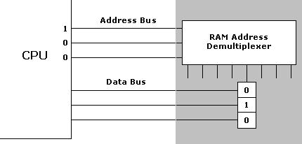
The CPU specifies the address on the address bus as a binary number
The RAM module internal demultiplexor activates that address -
In the above illustration the gray section represents the contents of a RAM module. The address bus can be thought of as a one way street. The processor places the address of the location that it wishes to read onto this bus. Devices do not signal the processor using this bus. The data bus can be considered a two way street in that the CPU can read data in from the location specified on the address bus or it can write data out to the location specified on the address bus across these wires. But these are still generally CPU driven. Devices will not signal the CPU across this bus, only render data if the CPU wants it or absorb the data on this bus if the CPU wants them to.
-
On the original 8088 the address bus was 20-bit and the data bus was 8-bit. This 8-bit data bus is why the 8088 was chosen over the true father of all x86 CPUs: 8086. The 8086 had a 16-bit data bus which allowed the system to make a single memory access on a single instruction cycle that could fill its 16-bit wide registers with a 16-bit wide number. In the 8088 since it had a chopped down 8-bit data bus, there had to be a two-step memory address process over multiple cycles each reading 8-bits of the 16-bit value being read into the register onboard the CPU. This made the PC at least twice as slow as a machine using the 8086. The 20-bit or 20-wire address bus allowed the 8088 to address a total of:
220 = 1,048,576 distinct addresses of RAM since each location stores 1 byte the total amount of RAM is then: 1,048,576 addresses X 1 Byte/address = 1,048,576 Bytes = 1MB -
These two buses (the address bus and data bus) are the primary buses around which the PC and indeed all computers operate. In modern systems there are more than one address bus and data bus to facilitate the high speed cache and the main peripheral expansion bus but they function exactly as explained here. This raises the third major bus found in the PC: the expansion bus.
-
The expansion bus is actually a large collection of buses and control lines to which peripheral components are attached to the system. The expansion bus also has expansion slots attached to it so that new peripheral components can be easily attached to the PC. The first expansion bus available on the PC was the
ISA – Industry Standard Architecture – bus. This early ISA bus featured an address bus width of 16-bits or wires and a data bus width of 8-bits or wires. It also included DMA channel control lines, IRQ control lines, +5VDC and ground lines to provide power to the expansion cards, and clock signals for the peripherals to synchronize with the activity of the CPU and to be able to tell when the address and data buses were holding meaningful information. The ISA bus was a scaled down standard expansion bus that was already in use on small computer motherboards and had a row of 31 contacts down each side of the connector giving it a total of 62-pins. -
The ISA bus was not renamed in the IBM AT even though it was dramatically overhauled. The new ISA bus for this system was extended and supports a 16-bit wide data bus and additional DMA and IRQ lines. The new ISA bus for the IBM PC runs on a standard clock frequency of 8.33Mhz while the original ran on a clock frequency of 4.77Mhz. These speeds match the clock frequency of the CPU's. The 8088 ran at 4.77Mhz as did the original ISA bus with the 8-bit data bus. The 80286 CPU introduced in the IBM AT ran at 6Mhz and later 8.33Mhz as did its new 16-bit wide data bus equipped ISA bus. This bus is sometimes referred to as the AT bus to distinguish it from the original ISA bus, but both names are commonly used for it and the PC repair technician should be aware that the original was slower and had only an 8-bit data bus within it. While the ISA bus is certainly deprecated, it was around for so long and lingered all the way into the Pentium III based systems that it is still found in millions of machines still in service, so the PC repair technician should be able to identify these expansion bus slots and be able to service these expansion cards. A small ISA bus is still the foundation of the expansion bus architecture even in the latest systems although the expansion slots are no longer available.
-
Physically the original slot was shorter and equivalent to the front section of the slots of the AT version of the bus. This makes the bus backwards compatible so that older cards could still be plugged into the front section of the AT bus slots. Some would still not work because of the speed of the new bus, however. The extension section on the rear of the AT expansion slot connector adds 18 more contacts to each side of the slot for a total of 98-pins. The IBM AT also introduced the full 16-bit wide data bus to the CPU eliminating the old chopped down 8-bit data bus used in the original 8088 based IBM PC.
-
The 80286 was the first protected mode capable processor by Intel. It is also the first CPU capable of running in real mode. This means that it can address memory exactly like the 8088 and in fact can run any program written for the 8088. Any non-8088 doing this is said to be in real mode, but it can also switch into its own native mode for RAM access which is totally different and requires programs written especially for it. This is called protected mode and the protected mode memory addressing capacity of the 80286 uses a 24-bit wide address bus introduced on the IBM AT.
-
The PC suffered some growing pains in the 1980's. The ISA bus was too slow, and many expansion cards needed a faster bus across which to transfer data with the CPU and RAM. Two different expansion buses emerged in the PC: EISA and the VESA Local Bus or VL bus. The Video Electronics Standard Association to which the PC video card manufacturers belonged were interested in bringing full screen animation like that of arcade video games to the PC. In order to be able to manipulate such a large amount of data in real time on screen a much faster bus was needed. They developed the VL bus for this purpose.
-
The VL bus as its name implies is attached directly to the front side bus and is therefore in direct contact with the CPU and the high speed pathways to RAM. Because of this, it has a 32-bit data bus pathway and can function in a synchronous mode moving 32-bits per clock cycle. This makes VL bus attached peripherals extremely fast compared to the alternative location on the ISA bus. Because the VL bus is bypassing the motherboard chipset, the video cards must be manufactured to extremely high quality and basically offer the functionality of the motherboard chipsets themselves making them at first very difficult to make. Since the front side bus speed of the 80486 was not fixed, some video cards would work on slower FSB's but not the faster ones. Some systems offered more than one physical VL bus slot, but this was intended to allow for the positioning of the physical expansion cards, not for the installation of more than one VL bus card which would more than likely crash the CPU if not actually damage it. The VL bus lines were designed for direct interface with the 486 CPU, when Intel introduced the Pentium CPU, it functioned so dramatically different from the 486, that the VL bus could not be adapted for the Pentium processors forcing it into obsolescence, a dangerous occurence in the PC industry and wasting years of development and expenditure on the technologies.
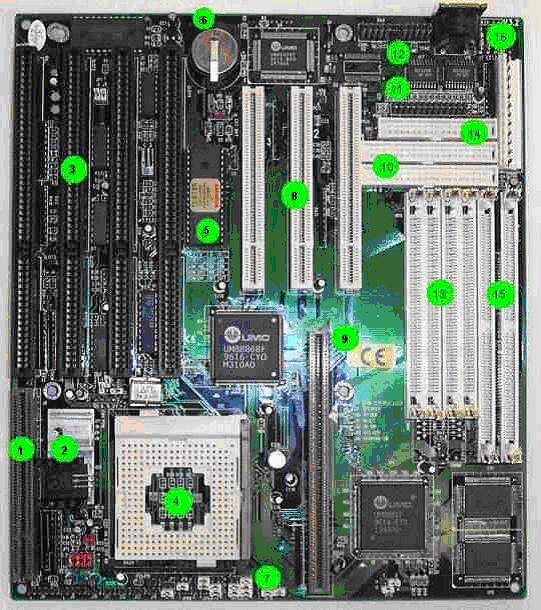
Components Indicated - VESA Local Bus slot
- Voltage regulator module for the processor
- 16-bit ISA slots
- 486 processor socket
- BIOS ROM chip
- BIOS battery CR2032 type
- Motherboard jumpers for selecting bus speeds processor voltages, etc.
- 32-bit PCI slots
- COAST - Cache On A STick slot for adding up to 256KB of L2 cache
- Dual 40-pin male IDC for connecting data ribbon cable for EIDE hard drives
- Male pin header for attaching a parallel port connector
- Two male pin headers for attaching serial port connectors
- 30-pin SIMM RAM module slots
- 34-pin male IDC for connecting the Floppy data ribbon cable
- 72-pin SIMM RAM module slots
- Dual 6-pin AT power supply-to-motherboard connectors
-
EISA - Extended Industry Standard Architecture, was developed around the same time as the VL bus and was another attempt to create a second generation 32-bit general purpose expansion bus for the PC industry. It is another extension of the classic ISA bus. This time a second row of contacts on each side exists within the connectors below the original rows of contacts. EISA provides a 32-bit wide data bus pathway and some rudimentary "Semi-Plug-n-Play" configurational capabilities. But it is still very much ISA in nature meaning that it is still an asynchronous bus taking anywhere from 2 to 10 clock cycles to make a single data transfer and it is still running at 8.33Mhz as a baseline although some custom chipsets could run it at 10Mhz or even 12Mhz, but this would usually cause the other regular ISA cards to fail, thereby defeating its purpose of being backwards compatible.
EISA Network Interface Card, the vertical second row of
edge connector contacts for the deeper EISA slot is clearly visible -
In the midst of this confusion IBM released a whole new product, the PS/2 (Personal System Type 2) line of personal computers. These were "parallel compatible" systems that could run all of the software designed for the PC and the AT. But they featured a new unique expansion bus: MCA - Microchannel Architecture. This bus ran at 10Mhz, it was sychronous (allowing each trasfer to occur in one clock cycle) and it offered 16 and 32 bit expansion slots. It was also "semi-Plug-n-Play" such that its ground work was the basis for the design of the EISA bus functionality. However, IBM protected MCA with patent and licensure and third party vendors had to pay very high licensure in order to manufacture expansion cards for MCA. It was a very expensive technology and it was a closed architecture that did not allow for free market competition to bring the quality of the products up while bringing the prices down. MCA and the entire PS/2 product line would fail due to its exhorbitant pricing by 1990 and cost IBM its majority market share as well: it does not pay to patent in the PC industry!
-
Because of the problems with EISA, VESA Local bus and MCA, each failing for a unique reason, Intel decided to invest their resources in developing a new high speed expansion bus especially because of their own plans to introduce the Pentium processor which would be extremely fast and powerful, and should not be bogged down by the old ISA bus interface with its peripherals. They developed the new high speed expasnion bus and published as an open architecture technology, free for all manufacturers to use, called PCI.
-
The PCI – Peripheral Component Interconnect – expansion bus of the modern 486 and Pentium generation systems is also an expansion bus that contains the address bus and the data bus just like the ISA expansion bus. The PCI bus is decoupled from the main FSB - front side bus like the ISA bus. The front side bus is defined as the lines that actually attach to the pins of the CPU itself. The FSB therefore runs very fast and also supports extremely short data states and extremely weak current representing the data states. Because of this, special groups of circuitry chips are used to translate data states between the CPU and the expansion slot attached devices so that they will not miss very short duration data states or very weakly signaled data states from the CPU and to protect the CPU from very long data states or very high current signaling from the expansion devices that could damage the CPU. These groups of specialized chips that bridge the speed and current gaps between the peripherals and the CPU are called the motherboard chipset.
-
Despite this decoupling, the PCI bus is similar to the ISA and indeed all expansion buses in that it carries the address and data bus lines to and from the CPU allowing communication between the CPU and all other devices. Also, despite the fact that the PCI bus is decoupled from the FSB it is often referred to as a mezzanine bus or even a "local bus" indicating that it is in direct contact with the CPU which is, technically speaking, false. The terms come from the fact that PCI, however, runs at 33Mhz and is therefore much faster than its predecessor. PCI also features a 32-bit wide data bus thus modernizing it to match the modern fully 32-bit CPU's from the 80386 to the Pentium generations. Finally the PCI bus is fully Plug-N-Play compatible meaning that as long as the expansion card and the motherboard chipset and the BIOS and the operating system are all strictly adhering to the standard, then the system should be able to identify the card, assign resources, and manage the installation of the drivers for the device automatically.
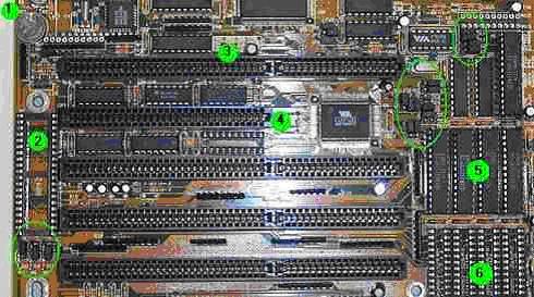
Components Visible Here - CR2032 standard CMOS battery
- Empty BIOS ROM DIP socket (chip has been removed)
- 16-bit ISA expansion card slot (notice the added right hand segment)
- 8-bit original ISA slot (notice it is missing the right hand segment)
- High speed Static RAM cache memory chips in DIP sockets
- Empty DIP sockets where additional SRAM cache chips could be added
- (Circled areas) – Jumpers for configuring the motherboard
-
In this image the original 8-bit (data bus section) ISA slot is to the left of the (4) and the one slot above it and the three below it are all the extended 16-bit versions. Since these were introduced on the 80286 based systems around 1983, these 16-bit slots should be the only type of ISA slot the modern technician will encounter. In fact within the past few years (2002 and beyond) this 16-bit ISA bus has also been phased out and is no longer available on modern motherboards and the cards are no longer manufactured except by specialty legacy device supporting companies.
-
ISA is an asynchronous bus meaning that the devices can execute interrupts at any time and contend with each other. The bus also supports 8-bit or 16-bit data transfers which introduces further device synchronization problems. ISA takes a minimum of 2 clock cycles to make a single data transfer across the bus and can take as many as 10 clock cycles to make a single data transfer. Since it runs at 8.33Mhz (millions of cycles per second) and takes at least 2 cycles to complete a data transfer (8.33Mhz ÷ 2 = 4.17Mhz) and each cycle can carry a 16-bit (2 byte) piece of data then the maximum theoretical data throughput of this bus is: 8.33Mhz ÷ 2 x 2 = 8.33MB/sec. ISA never actually achieves this throughput because of its asynchronous nature.
-
PCI as already stated has a 32-bit wide data bus and runs at 33Mhz and was designed specifically to replace the slow and aged ISA bus. It is a Plug-n-Play bus meaning that the devices attached to it can automatically negotiate system resources with the machine or their drivers can assign them after the operating system loads. The PCI bus is a synchronous bus meaning that all devices contend for the bus in a cooperative manner. Data transfers cross the PCI bus in one clock cycle and since the bus is synchronous, it can achieve the full throughput for bursts: 33Mhz x 4 bytes/transfer (32 bit data bus width) = 133MB/sec. This makes the PCI bus more than 16 times faster than ISA. The PCI bus specification is a 32/64-bit data bus width technology. The PC industry chose to implement the 32-bit version as the standard. The standard 32-bit PCI slot connector has two rows of 62 contacts each for a total of 124 pins. The contacts are much finer than the ISA ones so the connector is actually physically smaller than the ISA slot. The 64-bit PCI slot connectors have two rows of 94 contacts each for a total of 188 pins.
-
The standard form factor for the ISA card is 4.2" (106.68mm) high, 13.13" (333.5mm) long and it is allowed a maximum width (occupying one slot) of 0.5" (12.7mm). Many ISA cards are physically much smaller than this. The PC/XT card height of 4.8" makes them too tall to attach into the AT expansion slots and this height was eventually abandoned for the standard height of the IBM AT case slots. The standard PCI card form factor is the same since it was designed for the AT case as well but cards of this size are very rarely seen.
-
So far the various industry standard buses have been explored and the motherboard has been necessarily mentioned and shown. Now this component should be formally defined:
Definition: Motherboard - the main circuit board providing the platform for the PC.
-
The three main functions of the motherboard itself are:
1) Provide a socket or slot for mounting the CPU to the computer.
2) Provide the foundation for mounting the necessary circuitry (the chipset) to interface with the CPU.
3) Provide the foundation for the circuitry (the bus controllers) and the sockets and/or slots for the interface and attachment of optional peripheral components and RAM to the system. -
Motherboards come in various industry standard form factors two of which have already been mentioned in Lecture 5 - AT and ATX. In actuality the true AT form factor is physically quite large and was replaced by the "baby-AT" form factor. These motherboards were more compact with dimensions of 8.57" wide by 13.04" deep, but not all "baby-AT" motherboards adhere strictly to these dimensions either. Which brings up an important point: the "baby-AT" motherboard form factor was not a strict standard except in the positioning of the screw holes and expansion slots so that it could be mounted to the case.
-
The overall layout of the "baby-AT" was also not strict although most manufacturers placed the CPU mount near the far left front. The rest of the components could end up anywhere on the motherboard. AT motherboards can fully start up and function without any of the front panel connectors attached because the AT power supply has a physical throw on/off switch. Because of this, when the power uspply is switched on, it immediately sends power to the motherboard which starts up the PC.
Components Indicated - ISA bus slot
- BIOS EEPROM, DIP package in DIP socket
- BIOS battery connector, camera CR2032 type.
- PCI bus slot
- Main motherboard chipset components
- Processor slot, Super Socket 7
- Primary and Secondary ATA controller's IDE cable connectors
- Floppy Drive Controller's floppy cable connector
- AT power supply connector.
- AT keyboard connector
- L2 SRAM cache chips
- 72-pin SIMM slots
-
The ATX specification also defines precise screw hole positions and expansion slot positions so that the motherboard will mount directly into any ATX case and expansion cards will line up properly with the expansion slot openings in the rear of the case. However, the ATX specification does define regions of the motherboard where certain items should be located and in general the manufacturers adhere to the standard well. ATX motherboards will not start up or function unless some if not all of the front panel connectors are properly attached to them. This is because the motherboard circuitry is what ultimately signals the power supply to turn on, not the switch which only sends a signal to the motherboard to do this. The full ATX motherboard form factor is 12" wide by 9.6" deep.
-
The improvements over the "baby-AT" and other predecessors are:
- Standard I/O rear panel - This region is both flexible and roomy so that manufacturers have a convenient location where they can place all external connector ports and provide a standard sized cutout plate that mounts to the case eliminating problems with lining up various collections of external connectors to various cases.
- Single keyed power supply connector - Eliminated the possibility of connecting the power supply connector to the motherboard backwards which was usually catastrophic in the AT.
- Moved the CPU and RAM - The CPU was moved to the far rear right region of the motherboard next to the power supply, this allowed the power supply's pressurizing fan to blow across it improving cooling. Also by moving the CPU and its growing heatsink/Fan assembly to this region got it out of the way of full sized expansion cards.
- Standardized Internal I/O connectors - These are the connectors for the FDD and HDD data ribbon cables which were never fully standardized in the AT. Sometimes these would be located between expansion card slots and were often quite difficult to reach or even use. In the ATX these connectors have been given the front edge of the motherboard as a standard region making them easily accessible and keeping them from having the data ribbon cable drape over the rest of the motherboard obstructing access to the rest of the components.
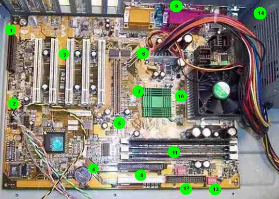
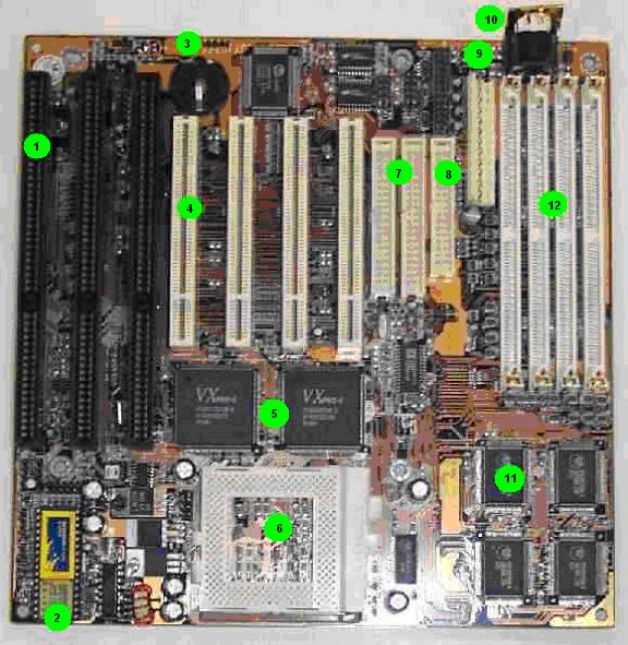
Components Indicated - CNR (Communication/Networking Riser) slot
- Front panel connector block pin jumpers with front panel cables attached
- PCI slots
- BIOS CR2032 type Battery
- AGP slot (Standard 1x/2x type)
- 20-pin keyed ATX power supply-to-motherboard connector and CPU fan connectors
- Major motherboard chipset component under a heatsink
- ATA controller connectors
- Rear panel connectors
- AMD 650Mhz Athlon/Duron CPU underneath a large heatsink/cooling fan
- PC100/133 SDRAM DIMM slots, top one has a 64MB PC100 DIMM in it
- Standard FDC connector
- Motherboard DIP switches
- ATX Power supply
-
The overall beneficial effect realized by the ATX specification is:
- Greater flexibility in the motehrboard design concerning integrated peripherals - Due to the standard rear panel and the accompanying plate the motherboard can provide many different built in peripherals and still fit into any ATX case.
- Ease of maintenance - The CPU and its massive heatsink/fan assembly no longer blocks full form factor internal expansion cards, internal drive data ribbon cables no longer obstruct the motherboard.
- Superior cooling - Due to the positioning of the CPU next to the power supply and its use of a pressurizing cooling fan.
- Reduced manufacturing cost - External connector ports can all be integrated within the standard rear panel area rather than have to have cables and rear slot connectors like in the AT based systems.
-
While the ATX specification was formally a power supply specification it also encompasses the design and layout of the motherboard and the case chassis as well.
-
The motherboard as stated provides the mounting system for the CPU, therefore one must decide on the CPU while choosing the motherboard. Modern systems provide Socket 478 or Socket T (LGA775) for Intel Pentium 4 and other "Family 15" products for the end user which include Pentium D, Pentium Extreme Edition, Pentium Core architecture processors including the Core 2 Duo, Core Solo, Core 2 Extreme and Core 2 Quad processors.
-
However, it is the chipset that will determine whether the system actually supports the CPU that has been chosen as much so as the CPU mounting system. The chipset will also determine the type and amount of RAM that is supported. Modern systems support DDR SDRAM, DDR2 SDRAM, and dual channel DDR, and dual channel DDR2 for the most part. The chipset will determine which type of main memory system is supported and the speed of the actual memory modules that must be installed onto the motherboard.
-
Since ISA is no longer offered on modern systems, they will for the most part offer PCI as the general purpose expansion bus and either AGP or PCI-Express x16 slots for the video controller. Modern systems also offer SLI - Scalable Link Interface, in which two graphics cards can work together rendering the images on a single screen effectively doubling the performance over a single card. The motherboard, the video cards and the drivers must all support this.
-
As mentioned ATX motherboards can offer a variety of integrated peripherals. Almost all ATX motherboards offer:
- Keyboard controller - dual PS/2 type connectors for keyboard and mouse.
- Dual Serial Ports - Usually with Male DB9 connectors, this technology is becoming deprecated.
- Single Parallel Port - With a female DB25 connector, this technology is becoming deprecated.
- USB Host Controller(s) - With at least 2 female "A" ports.
- Floppy Disk Controller - With a single 34-pin male IDC near the front edge of the motherboard. This technology is deprecated.
- ATA (Advanced Technology Attachment) Controller - For attaching EIDE hard drives. Parallel ATA technology usually provides two 40-pin male IDC but is becoming deprecated in favor of Serial ATA (SATA) which usually provides 4 or more SATA connectors for hard drives.
-
Optional peripherals that motherboards can also include easily with the ATX design are:
- Sound Controller
- Video Controller
- Internet Connectivity Device
- FireWire Controller
-
Clearly then one could purchase a motherboard that has all of the peripheral devices necessary to function as a complete working PC, except of course for the CPU, and RAM. Adding a hard drive and optical drive and the PC would be complete. While these optional integrated peripherals are certainly not the quality of standalone expansion cards they are adequate for basic computing tasks. A "PC in a motherboard" would cost far less than assembling a PC out of all of the separate components and the component compatibility is not an issue since the manufacturer has already dealt with these issues for the most part in integrateing them int othe motherboard. For basic, simple microcomputers, these fully featured motherboards are a bargain, but they are not intended for performance demanding applications like video games, engineering workstations or network servers.
Review Questions
-
Define a circuit bus:
-
If a processor has a 16-bit address bus, how much RAM does it support?
-
What is the highest address on a 16-bit address bus?
-
What was the maximum theoretical throughput of the original 8-bit ISA bus? What does the "8-bit" refer to in this question?
-
Which of the 2nd generation 32-bit expansion buses discussed in this module was proprietary (closed architecture)? What effect did this have on the prices of the technology? What ultimate effect did this have on the manufacturer? Who was the manufacturer?
-
Which of the 2nd generation 32-bit expansion buses discussed in this module was yet another attempt to extend the ISA bus? What was its major shortcoming?
-
Which of the 2nd generation 32-bit expansion buses discussed in this module was the most difficult to manufacture expansion cards for? Why was this? What caused this bus to be shortlived?
-
Which of the 2nd generation 32-bit expansion buses discussed in this module succeeded by avoiding the shortcomings of all of its predecessors? Who developed it and why?
-
How many contacts in the original 8-bit ISA slot? The 16-bit AT bus slot? The 32-bit PCI slot?
-
What is the speed and data transfer width of the standard PCI bus? What is its throughput?
-
What is the throughput of a VL bus slot attached to a 33Mhz FSB?
-
Define motherboard:
-
Name the three main functions of the motherboard:
-
List and describe the main features of the ATX motherboard layout.
-
List and describe the benefits of the changes made to the ATX motherboard layout:
-
List two types on modern CPU socket mentioned and list the CPU's that they support.
-
List four different RAM memory systems that are found in modern motherboards based on their chipsets.
-
List 6 standard peripherals built into ATX based motherboards.
-
List 4 additional peripherals that can easily be included in modern ATX motherboards.
-
Is it possible for an ATX motherboard to have all peripherals needed by the MPC '97 specification except for the drives? What is the main advantage of such a motherboard? What is the main disadvantage of such a motherboard?
-
Based on the images and parts lists what seems to be a common type of BIOS battery?
-
What type of package is the BIOS chip on most systems?
-
VL bus slots are unusual because they are located directly behind what other type of expansion bus slot?
-
List the three industry standard open architecture bus slots mentioned in this module designed specifically for video cards? Name the modern technology that allows two physically separate video cards to work together rendering the images on a single display.
-
What is the maximum amount of RAM that an 80286 processor can support?
-
What does the term Plug-n-Play mean?
-
What expansion bus is called a mezzanine bus? What is this referring to? Why is it technically incorrect to refer to this bus as a local bus?
-
What bus does the CPU directly attach to?
-
What are the dimensions of a standard form factor PCI card?
-
Which 2nd generation 32-bit expansion bus described in this module was the only fully backwards compatible expansion bus in that regular ISA cards would work in it?
-
Which 2nd generation 32-bit expansion bus described in this module was the only expansion bus that lasted a single generation of processors? Which processor was it designed for and completely dependent on?
-
Which motherboard form factor was developed together with its power supply?
-
Which motherboard form factor repositioned the CPU so that the power supply fan could cool it as well as ventilate the entire system?
-
Which motherboard form factor featured a standardized rear panel for positioning integrated peripheral external ports? This allows such motherboards to fit into which case chassis?
-
When selecting a motherboard which three other types of components choices will be decided by its physical components?
-
Which motherboard will not function until at least some of its front panel connectors are attached properly? Which type of motherboard based system will start up and function without any front panel connectors attached to it?
Copyright©2000-2007 Brian Robinson ALL RIGHTS RESERVED