CET1171 Lecture #7 - Processors
Materials: Working complete PCStudent bootable floppy diskette - "New Boot A Version 2"Student bootable CD-ROM Working complete PCStudent bootable floppy diskette - "New Boot A Version 2"Student bootable CD-ROMObjectives: List and describe the entire intel x86 family including,Each CPU's features and capabilities,Each CPU's limitations,Be able to identify which CPU is installed in a system,Know the RAM associated with each generation of CPU,Competency: The student will be able to determine which CPU is installed in the system. The student will be able to identify the RAM technology requirements for the system and be able to run diagnostics for the CPU, and RAM. |
-
Boot up the PC. Due to the large number of PCI devices in the device listing of the text mode BIOS screen the CPU type always scrolls out of view. This will probably be the norm on late model PCs. Enter the BIOS and disable the Quick Power On Self Test feature. When you reboot the BIOS will perform a memory count. During this phase hit the Pause/Break key. Now record the processor type, total amount of memory and the BIOS serial number across the bottom of the screen. This serial number can be researched on the web to determine if the system already has the latest BIOS update for use in the lecture module concerning the system BIOS.
-
Start Windows in Normal mode and Right click on My Computer and select properties. Make a note of the processor and RAM reported. This only reports RAM amount but not the type. Under this "General" tab of the system properties sheets the processor is also listed. In the case of later versions of Windows and Intel CPU's the family and steppings are indicated. Record these values then go to the Microsoft and Intel websites and determine the processor based on this information.
-
Now click Start > Run and type "MSINFO32" into the text box then click the OK button. In the start up right pane the processor type is indicated. Record this. Note that the OS does not provide comprehensive information concerning the identification of the processor for the user despite the fact that it must identify the processor in order to load appropriate versions of the OS kernel.
-
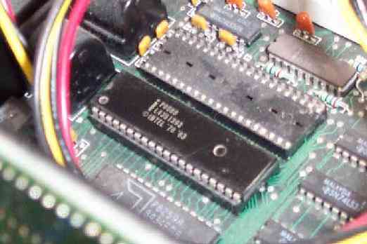
Find the CHKCPU.ZIP utility on the Student CD-ROM. This is a free download from the Internet and we should all be thankful to Mr. Steunebrink for his contribution to the world. Unzip it to the HDD and open a DOS box and run it. Record its output information in the module below. Note that the program cannot reveal the clock multiplier while in Protected mode. Restart in MS-DOS mode and run the program again to get this information.
C:\BIN>chkcpu CPU Identification utility v1.9 (c) 1997-2002 Jan Steunebrink --------------------------------------------------------------------------------- CPU Vendor and Model: Intel Celeron 4 1700/1800 E0-step Internal CPU speed : 1714.3 MHz (using internal Time Stamp Counter) Clock Multiplier : Available only in Real Mode! CPU-ID Vendor string: GenuineIntel CPU-ID Name string : Intel(R) Celeron(R) CPU 1.70GHz CPU-ID Signature : 0F13 |||+-- Stepping or sub-model no. ||+--- Model: Indicates CPU Model and 486 L1 cache mode |+---- Family: 4=486, Am5x86, Cx5x86 | 5=Pentium, Nx586, Cx6x86, K5/K6, C6, mP6 | 6=PentiumPro/II/III, CxMII/III, Athlon, C3 | F=Pentium4 +----- Type: 0=Standard, 1=Overdrive, 2=2nd Dual Pentium Current CPU mode : Protected Internal (L1) cache : Enabled in Write-Back mode C:\BIN>_ -
In order to understand how the IBM PC works it is necessary to understand that the PC is a computer system centered around the Intel 8088 CPU – Central Processing Unit. And that this CPU is in fact the computer itself. The rest of the PC exists for the purpose of allowing information to enter this computer, be stored by the system, be retrieved by the system, be processed through this computer, and to be displayed to the user. The computer that will be described here will be the 8088 microprocessor which is the ancestor of all of the subsequent CPU's developed by Intel for the IBM personal computer family of systems starting with the IBM PC, then the XT, then the AT. IBM continues to have a huge influence on the personal computer market despite the fact that their sales plummeted in the early 1990's and have currently fallen to practically single percentage figures.
-
One of the most important concepts for the PC technician to know about the processors that are the computer's at the heart of each successive generation of this family of personal computers is that up to the Pentium 4, they are ALL backwards compatible. This means that the Pentium 4 can execute 8088 executable programs and therefore understands 8088 machine language. The 8088 instruction set is a subset of the complete Pentium 4 instruction set. It can also therefore be said more accurately that the Pentium 4 instruction set is a superset of the preceding x86 family processor's instruction sets that trace all the way back to the 8088. Later we will see that the 8088 memory addressing scheme is completely different from the Pentium 4's also, because of this the Pentium 4 powers on or resets into 8088 emulation in which it is effectively nothing more than a very fast 8088.
-
When any CPU from the x86 family is running in 8088 emulation this is referred to as real mode (I suppose the term means it is acting like a real 8088?). When the CPU is switched from real mode into its native mode of operation, in the case of the Pentium 4 it is switched from acting like an 8088 to acting like a Pentium 4, then this is referred to as protected mode. This term refers directly to one of the main features of the way the native 32-bit CPU's manage memory which we will investigate later.
-
Because the machine starts up in real mode, all BIOS code is written for real mode (modern BIOSes are including more and more protected mode instructions), and all of DOS is written for real mode. There are a few exceptions in the later versions, DOS 6.22 includes HIMEM.SYS which does provide access to extended memory through a protected mode interface to any program that knows how to use this API – Application Programmer's Interface - which is written in the 80386 native instruction set. Therefore, learning the 8088 processor as the example has real world applicable value to the PC expert since so much code exists in modern systems for it and all modern CPU's reset to emulate it.
-
The activity of the 8088 CPU will be described partially in order to get enough of a grasp of the machine necessary for this lecture and it will not be fully described here since it actually quite a complex computer in its own right. The 8088 CPU has many 16-bit wide registers of several different categories of functionality, it has a 20-bit wide memory address bus and an 8-bit wide data bus. This narrow data bus is handled by the motherboard chipset transparently to the CPU so that it can be treated as if it were 16-bits wide. This is one of the main reasons that the 8088 was chosen over the 8086 which has a true 16-bit wide data bus which would have driven the price of the motherboard, chipset, and expansion cards costs so high that the system would not have remained affordable.
-
Each block of the registers is actually four binary bits wide. A register is simply a special set of circuits that can hold and also manipulate a large binary place value number. Since each block in the diagram actually represents 4 binary digits it can be seen then that the general purpose registers named "ax" and "bx" are actually 16-bits wide. As are the segment registers "ds" and "cs" as are the pointer registers "si and "ip"
-
The physical data bus register exists physically in the CPU but not logically. That is, it can never be referred to directly by the programmer in the machine language instructions and is under the exclusive control of the CPU itself. The same is true of the physical memory address register although the programmer can exert complete control on the registers used to calculate its value.
-
The diagram illustrates two of the 8088's general purpose registers named the "ax" and the "bx" These are where a number can be brought onboard the CPU in order for a mathematical or logical operation to be performed on it. If a program for this machine is to add two numbers together, the numbers must be brought onboard into these registers, then they can be added, then the result can be stored back out in memory. This is true of all of the x86 family processors from the 8088 up to the modern processors.
-
This diagram also illustrates two of the 8088's "segment" registers named the "ds" (data segment) and the "cs" (code segment). These are used to point to the place in memory where the data is stored (the ds) and to where the program that the machine is currently executing is stored (the cs). The 8088 has one more extremely important segment register called the "ss" or Stack Segment register which will described later.
-
This diagram also illustrates two of the 8088's "pointer" registers, the "si" (source index) and the "ip" (instruction pointer). The si register points to a particular address within the data segment of memory which the CPU would access. This is how the CPU will read a data value in, or write a data value back out to memory. The x86 family is certainly not limited to the use of the si register for this, it has many addressing schemes for accessing data in RAM; far too many to discuss here. The ip register points to the particular instruction that the CPU is about to fetch, then decode and execute within the program stored in the code segment of memory.
-
So at this point it is important to take a closer look at memory since it appears that this machine is going to be working with it quite a lot according to the above descriptions of the registers. In fact, the CPU must have memory in order to function and basically does nothing but execute programs loaded into memory, and read raw data that has also been loaded into memory, process this data and then write the results of this processing back out to memory.
-
The memory referred to here is RAM - Random Access Memory. This is an array of high speed digital electronic circuits that can store the binary numbers that are the numbers that the CPU works with. The CPU will treat some of these numbers as instructions for it to perform and it will treat others as data and information that those instructions have it manipulate.
-
The machine only knows which is which by having the proper program instructions loaded into the proper location in memory and by having the proper data values also loaded into the proper location in memory as well. The programmer's are entirely responsible when designing the programs for this machine that all of this will be done correctly and set up the programs and data in memory and set up the values in the segment and pointer registers so that these segment/pointer register combinations are pointing to the locations in memory that hold what they are supposed to be holding; the program that the machine is running should reside in the memory address pointed to by the cs:ip combination and the data being worked on by that program should be pointed to by the ds:si combination.
-
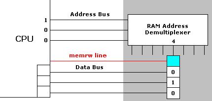
The address select line comes from the RAM address demultiplexer so that whatever binary number is represented on the address bus, the demultiplexer will decode it and activate one specific address select line, the one for the cell whose address matches the binary number on the address bus.
-
The state of the Read/Write select line coming to the cell is replicated from the state of the "memrw" line which comes directly out of the CPU. This is how the CPU indicates to memory whether it is reading from memory or writing to memory.
-
Each cell is individually connected to the data bus lines which run throughout the memory array. If the CPU is indicating address (00000000000000000)010 on the physical address bus, then the address select line to the middle cell of the illustration above would come on. If the CPU is attempting to read the data held in this cell, this would be indicated by the state of the Read/Write line at that cell as well and the address control circuit would switch on connections (transistors as we have seen) between the voltages held in the individual bit cells to the data bus wires thus exposing the contents of this particular memory cell to this bus. The CPU is also attached to these bus lines and would "catch" these voltages at the physical data bus register. This would complete a single RAM memory read activity.
-
If the state of the CPU's memrw line were indicating a write (note that the state of this line is either a "0" or a "1" meaning either a read of the cell or a write to the cell) then the CPU will place the number that it wants to store in the cell into the physical data bus register and then activate the set of switches (transistors) so that these voltages appear on the data bus lines. Then the address bus would indicate which cell is being written to and the demultiplexer circuits will select it. The state of the memrw line will indicate that the CPU is writing to the cell and so the address control circuit will clear the individual bits of the cell and again switch the bit cells so that they are in contact with the data bus. This time the cells will take on the voltages present on the data bus lines thereby storing the number they represent in the memory cell thus completing a CPU write to memory.
-
In the situation illustrated here, the CPU has placed the address "100" onto the address bus and the RAM demultiplexer circuit has activated the address select line for the memory cell #4 (100b = 4d):
-
The memrw line is indicating that this is a memory read so the address control circuit (the blue box) connects the individual bit cells of this RAM address to the data bus lines and the voltages appear on these wires. The CPU's physical data bus (register the boxes in the lower right corner of the CPU) can then "catch" these voltages.

-
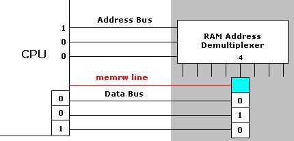
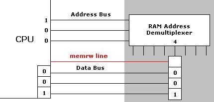
In the case that the CPU is writing to the RAM location, again the address of the location that the CPU wishes to write to is placed on the address bus and the RAM demultiplexer selects the memory location. Note that the CPU will also have the number that it wishes to write to this location staged in its physical data bus register:
-
At this point the memrw line indicates that this is a write from the CPU to the memory location. So the address control circuit (the blue box) will clear the bits and connect them to the data bus. The bit cells will absorb the voltages on these lines thereby completing the write to this RAM location from the CPU:
-
Examining this section of RAM it can be seen that each address will be activated only when the actual address number has been placed on the address bus by the CPU. The address demultiplexer circuit of the RAM chip will determine which unique address select line to turn on which of course will activate the desired memory cell. The CPU has an interface wire coming from it called the "memrw" line (memory read/write) the state of this line will also be forwarded to the cell control circuit so that the memory cell will either expose the voltages held in the individual bit circuits that make up the memory cell onto the data bus wires, effectively a read of its contents, or the bit circuits will absorb the voltage states on the data bus, effectively writing a number from the CPU to them. (Note that all of this is not totally literally true, but it is all close enough to the truth for a PC technician).
-
A memory loaction for the 8088 CPU consists of an address control circuit and the eight bit cell circuits connected to it that hold the byte that it can store. It can hold one 8-bit binary number that can be either one piece of an instruction of a program or one piece of data that the program will manipulate. The entire amount of RAM that the 8088 CPU can address (its maximum amount of RAM supported) is determined by how the segment registers and pointer registers are used. The 8088 uses a four bit shift to the left of the segment register then it adds the pointer to this. This sounds bizarre (and in fact it is), but by introducing the segment registers Intel made it possible for the 8088 to construct a number larger than the 16-bits held in its registers so that very large programs and/or very large amounts of data could be handled by the CPU. Let's assume that the code segment register currently holds the value 1000h and that the instruction pointer currently holds the value 2345h Now the CPU will shift the cs value four bits to the left and then add the ip register's value to this:
CS = 1000h, IP = 2345h
Remember that each hex digit is four binary bits so shifting the CS four bits to the left is the same as shifting it one hex digit to the left:
CS <- 1 hex digit = 1000_ Add the IP to it + 2345 12345h -
From this it can be seen that since the cs register is shifted four bits to the left that the code segment of RAM pointed to when the cs register is 1000h is actually 10000h and that the physical address bus is actually 20 bits wide. The highest 20-bit wide number is 11111111111111111111b = 1,048,575. So the maximum amount of RAM that the 8088 can address is 1,048,576 addresses (remember that 00000h is also a valid address and is the 1st address making 00001h the second and FFFFFh the 1,048,576th address). It is the physical address bus register that will be fed the current value of the segment and pointer registers when any RAM address must be read from or written to and it will automatically perform this bit shift and calculate the physical address and place it onto the address bus.
-
We also see that each memory cell's individual bit cells attach to the data bus whose wires ultimately lead back to the 8088 CPU's physical data bus register. When the CPU wishes to read a value from a particular memory location, the proper segment and pointer register values are given to the physical address bus register which calculates the physical address and places it on the address bus.
-
It is clear then that the voltages on these wires that are held within the bit cell circuits are synonymous with the binary number that they represent. What is not clear is that the transistors that make up these circuits do not know this. All of these circuits are nothing more than collections of switches simply responding to the inputs of the other switches and they change states and send voltages or lack of voltages or "on" and "off" states back and forth between each other. It is only the humans who have designed them to do this in a particular way that make these voltages take on the interpretation by humans as binary digits of value "1" or "0" Because of this it is interesting to note that in some circuits the lack of voltage can be assigned by the designers to mean "1" and the presence of voltage to mean "0" even though you would expect no voltage to mean "0" and some voltage to mean "1" Again it is the humans who assign these meanings, the circuits just switch themselves based on what the other circuits have sent them a signal to do.
-
Now that it is seen how the machine reads and writes values to and from RAM, it is possible to understand the full operation of the 8088 and the machine will be followed through the execution of a few machine language program instructions so that the student can fully understand this computer and how it works; in real mode for now.
-
As mentioned earlier the 8088 operates using three segment registers (although only two were illustrated to keep the diagram as simple as possible). The cs or code segment register is a 16-bit register that is actually shifted 4 bits to the left. Since 4 bits can count from 0 to 15 and these are demultiplexed into addresses, this means that the cs segment register could have the value 1234h for example, but shifted 4 bits to the left (one hex digit) it is really the number 12340h which is the physical memory address in RAM. Adding 1 to this register results in the number 1235h and after the 4 bit shift 12350h. So the cs register can only point to a specific address in RAM on even boundaries that occur every 16 bytes. These 16 byte gaps and the even cs numbers (like 12350h) are called paragraphs and paragraph boundaries.
-
With the cs register set to 1235h it is pointing at the RAM memory segment that begins at the physical address paragraph 12350h. If the ip register is 0000h then the physical address bus register will hold the value 12350h which is the lowest possible physical address that the cs:ip combination can address as long as the cs = 1235h. This then is the starting point or absolute bottom address of RAM segment 1235h.
-
If the ip register holds the number FFFFh, then the physical address bus register will add 12350h + FFFFh = 2234Fh. This would be the highest possible physical RAM address that could be accessed while the cs register stays set to 1235h and is therefore the absolute top address of the RAM segment 1235h. Subtracting the top address (2234Fh) from the bottom address 12350h yields: FFFFh which makes sense when one realizes that the range of addresses within the segment are spanned by the ip register which is 16-bits wide which is exactly the size of this number. Converted to decimal it is 65,535. Counting the zero address at 12350h as well yields 65,536 or 64KB. This is the size of a single RAM segment of the 8088 in real mode addressing.
-
A program can easily execute instructions in a variety of ways to change either the code segment or the data segment or even the stack segment to any value from 0000h to FFFFh and therefore is definitely not limited to a single 64KB segment of RAM. Any program can use any number of segments (note that they can be defined every 16 bytes and are 64KB deep so multiple segments can easily overlap often to the unwary programmer's dismay) and can access any physical address within the addressable megabyte spanning from 00000h to FFFFFh.
-
Armed with this background information, assume that the program has already been loaded into RAM and that the segment registers have already been initialized so that they are pointing to the correct locations in RAM. That is, the cs and ip pair are pointing to the first executable machine language instruction of the program that the CPU is about to fetch, decode and execute. In fact, the 8088 is totally nonfunctional without RAM and is a computer that is designed to fetch, decode and execute machine language instructions from RAM. It is designed to manipulate raw data stored in RAM and to generate output information in RAM. Interaction with other devices is quite a challenge since this computer essentially does nothing more than operate on numbers stored in RAM. Later the engineering solution of how the CPU was designed and how the PC was designed to allow input and output to peripheral devices will be discussed in detail.
-
The ds segment is pointing to the segment of RAM where the data that the program is going to manipulate and generate will be stored and the ss (Stack Segment) and sp (Stack Pointer) are pointing to the top of the memory stack.
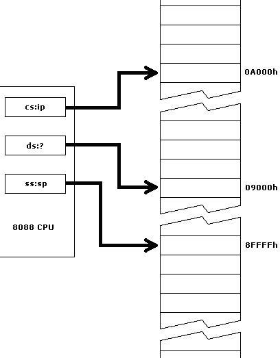
The three main segment:offset registers point to three physical addresses
in RAM at any given moment: the program it is executing, the data that
program is working on, and the stack where it can keep a note to itself -
Assume that the cs = A000h, the ds = 9000h and the ss = 8000h. Also assume that the ip = 0000h and the program is about to begin executing. Note the "?" next to the ds register. This is because the 8088 has many ways of addressing data using the ds as the segment register, it does not have to use the si in fact it can use a direct value within an instruction and most of the registers other than the segment registers as the pointer to the address within the data segment.
-
The sp or stack pointer's value is FFFFh which is why the current ss:sp pair point to the physical address 8FFFFh. The stack is nothing more than a special way of treating RAM which requires less overhead, but more planning on the part of the programmer. There are memory read write operations that are dedicated to the stack and many low level operations of the CPU depend on the stack in order to retrieve critical values such as the return addresses from long jump instructions. Picture the stack as the stack of dishes next to the dishwashing employee in a busy restaurant (hence the name "stack") The bus boys bring in 10 dishes and the dishwasher begins to wash them, first the top one and sets it aside, then he grabs the next one, which is the new one on the top of the stack washes it then sets it aside. Then he grabs the next one which is again the new one on the top of the stack washes it and sets it aside. Now he has cleaned 3 dishes and the fourth one that was brought in originally is now the dish on top of the stack. Now lets say that the bus boys bring in two more dishes. They will place them on the top of the stack. So now the dishwasher grabs the top dish (and notice that it just arrived on the stack) washes it and sets it aside. Now he grabs the next one, washes it and sets it aside. Now that fourth dish from the original group is back on the top of the stack. And the bus boys bring in 4 more and place them on the top of the stack.
-
So the stack is a type of memory called a LIFO – Last In, First Out. And it starts at the highest address of the segment and works its way down. It does not need a direct numerical address reference to function either. The dishwasher does not need to know the address of that fourth dish at any time, just how many dishes have been stacked on top of it at any given moment and he will know where it is. This is the power of the stack to the programmer. To the CPU it has a default behavior built into many of its instructions. When the processor is about to execute a jump that will change both the segment pointer and the instruction pointer carrying it to a distant location in memory, the CPU will automatically "push" the current cs and ip values onto the current stack position. This is a total of 4 bytes (each register is 16 bits or 2 bytes wide) and so the stack pointer which points to the current place on the stack that can be written to will be decreased by 4. As long as the distant part of the program does not alter the stack segment or pointer, a "return" instruction can be executed and it will simply "pop" the four bytes on the top of the stack off and place them into the cs and the ip effectively returning the program to where it started from before the jump and there is no need for the return instruction to refer to the original place in memory from which the CPU jumped from so it, nor the programmer have to know the actual value either. It may sound a little weird the first time you read it, but trust me it is very easy to code large programs for this machine without having to know the exact address every byte of the way through the program. Just write "Jump [to] procedure X" and at the end of Procedure X just write "return" and it works. But its not magic, the programmer has to be aware of exactly how the machine returns or he will mess up the stack not knowing that the machine needs it and then the program will crash (Despite knowing it, they seem to do a fine job of crashing it anyway!)
-
At this point the technician should be aware of how the 8088 CPU works at the fundamental level reading and writing to RAM. The technician should note that any program for the 8088 keeps three physical addresses: the place where the actual machine language program instructions reside in RAM pointed to by the cs:ip pair, the place where the raw data resides in RAM pointed to by the ds:si pair (as one example pointer register), and the stack where the CPU can automatically store long jump return addresses (and many other things) pointed to by the ss:sp pair. The technician should be aware that the CPU does not "know" the difference between program code and data. This is the responsibility of the programmers to position it in RAM properly and to set up the segments and pointers properly. This is the exact job of the operating system. When the user runs or executes a program, by typing its name at the command prompt, or double clicking its icon in Windows, the operating system reads the program file off of the drive and into RAM, sets the segment:pointer pairs properly and then the program begins to execute.
-
The evolution of the x86 family started before the first IBM PC model. The original 8086 processor was actually too expensive for the PC which as each successive design problem was solved was steadily growing in price such that it was going to become too expensive to be a feasible "personal computer." IBM therefore decided to base the original IBM PC on the Intel 8088 processor, a much cheaper variant in which the data bus attachment to the external bus was cut down to 8-bits wide rather than 16-bits. This allowed the data bus through out the PC to be made 8-bits wide rather than 16-bits which made the manufacture of everything from the motherboard to the expansion bus slots and cards cheaper. The 8088 chip was also much cheaper than the full blown 8086. However, the chip is still a 16-bit CPU meaning that its registers can hold 16-bit numbers and it can perform internal mathematical and logical calculations on those 16-bit numbers. Because the data bus is cut down to 8-bits wide on the IBM PC and the 8088 CPU, each memory fetch requires two complete fetches to fill a register instead of one. This makes the 8088 based system immediately twice as slow as an equivalent 8088 based system all other factors begin equal.
Original 8088 Microprocessor within an IBM PC, open 40-pin DIP
Socket next to it is for the 8087 Math Coprocessor. -
Intel would develop a successor to the 8088 called the 80186. It was technologically more advanced but still had a 16-bit data bus like the 8086, and still ran 16-bit machine language yet it was far more expensive than the 8088. IBM decided to pass on the processor which Intel was banking that they would buy. Intel would scurry to develop a much more powerful step up from the 8088 and released the 80286 shortly afterwards.
-
This processor still features 16-bit registers and is fully backwards compatible not only capable of running machine language programs written for the 8088/86 but also in fact completely emulating it at power reset. However, the 80286 is a different CPU and can be switched out of the 8088/86 emulation mode called real mode into its native mode called protected mode in which it still shares a common set of machine language instructions with its predecessors. But it also has its own new superset of instructions and powerful new memory addressing schemes allowing programs to access up to 16MB of RAM instead of the old 1MB limit of the pure 16-bit 8088/86 instruction set and functionality. The 80286 memory addressing schemes also allow the processor to allocate a fixed block of memory to an application and if that application attempts to execute an instruction that addresses a memory location outside of that range the CPU will automatically throw an interrupt and execute the interrupt routine instead. The operating system designers can place OS functions in this interrupt and a protected mode CPU management interrupt is called an "exception" or a "fault." When it concerns programs violating protected memory spaces it is called a general protection fault.
-
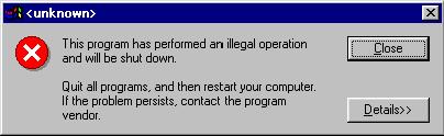
Windows kernel operating system code is written in two fault mode levels, if the OS kernel determines that it is still undamaged by the fault it will open the ubiquitous "This program has performed an illegal operation and will be shut down [OK]" window. If the OS determines that the kernel itself may be compromised it will switch the video card back to text mode and issue an infamous "Blue Screen Of Death" error message and more than likely lock up the system at this point. The '286's vastly improved speed (10-12Mhz) and memory addressing capacity was enough to attract IBM. While they were modifying the motherboard to accommodate the new CPU they decided to introduce more motherboard improvements intended to overcome nagging shortcomings of the original PC's design. The result was the IBM AT.
-
The IBM AT included the following architectural changes:
- 16-bit data bus from CPU to the rest of the system including RAM, expansion bus
- 16-bit data bus expansion to the ISA bus slots, old cards still work in them
- Added a second PIC – Programmable Interrupt Controller providing a total of 15 IRQs (1 attaches the "slave" PIC to the original "master") instead of 8
- Added a second DMA – Direct Memory Access controller. Each DMA actually has two lines, the DMA Request and DMA Acknowledge so the second contoller adds 4 new DMA channels one of which is unavailable and attaches it to the original. The second DMA supports the 16-bit data bus.
- Added the RTC – Real Time Clock, so that the system can retain the Time/Date internally while off and because this chip had 64 bytes of RAM built into it:
- Added the BIOS Setup Utility for software configuration of installed hardware which stores the hardware configuration in the RTC chip's CMOS RAM
-
Before the IBM AT, that would be the IBM PC and XT, there was no RTC chip on the motherboard, therefore the system did not retain the Time/Date and these had to be manually entered every time the machine was turned on. And because there was no RTC chip, there was no CMOS RAM either, so the BIOS could only be configured through jumpers and DIP switches on the motherboard. Adding RAM, upgrading or adding a second floppy all required setting jumpers or DIP switches on the motherboard or the system would not recognize the hardware or worse: cause a POST failure until the settings were corrected to match the hardware configuration.
-
The BIOS Setup Utility and the CMOS settings allows the user to change the hardware, then run the utility and make the changes in software from menu choices which are plain and clear on screen, whereas jumper settings and DIP switches are generally marked with something like "JP1" on the motherboard and it is absolutely not clear what this jumper sets. The inclusion of the RTC chip and the CMOS RAM for holding hardware configuration that is set through the BIOS Setup Utility was a huge advance that changed the PC from more of a "hobbyist toy" into a "real" computer especially since the machine retains the Time/Date which are critical to the workplace environment.
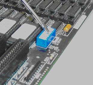 Setting DIP switches on the motherboard
-
Intel's next processor the 80386DX would be released in late 1985. It would be the first full 32-bit CPU intended for the PC market. It featured 32-bit wide registers allowing te chip to perform native machine language operations on 32-bit numbers for the first time. The 386 has a large new superset of instructions to accommodate these operations. Like the 286 the 386 will power reset into real mode and must be switched into protected mode. A major difference is that the 386 can be switched back into real mode without having to reset (reboot) the machine. This is one reason that HIMEM.SYS is able to make extended memory available to applications that know how to call it because it switches the system into protected mode accesses extended memory using 32-bit native 386 instructions and then switches back to real mode then passes control back to the 16-bit DOS program or the 16-bit DOS kernel. The 386's protected mode functions differently from the 286 in memory addressing details but is backwards compatible. The new 32-bit IP (instruction pointer) register allows the 386 to address 232 memory locations or 4 Gigabytes of RAM. To put the power of the 386 in perspective, it was released in 1985 capable of running 4GB sized programs in RAM, yet as of this writing, 20 years later the standard PC still does not come with this much RAM.
-
Another major feature of protected mode is the processor's capability that is referred to as multitasking. There are two types of multitasking that have been developed to take advantage of this feature of the processor: cooperative multitasking and preemptive multitasking.
-
In multitasking the CPU can effectively stop the execution of a particular program and push all of the current values in all of the registers onto the stack and read in all of the values for all of the registers of another program in progress from the stack. This means that the execution of one program can be interrupted and saved onto the stack in RAM and another program that was saved in the middle of execution can be read back off of the stack and continue to execute where it left off. Multitasking can handle several programs executing this way and move through them one at a time giving each a small amount of time to execute on the CPU and then stop the program, save the state of the CPU to the stack and reload the next one. Then it can stop and save the state of this next one onto the stack and pull the next one off of the stack until it has given each program a time slice.
-
Once all of the programs have had a time slice the first program gets to execute again for a short time and this process continues in a round robin fashion constantly. If a program ends it gets removed from getting a turn. If another program begins it gets inserted into the rotation. All of this happens so quickly, the changing from one program to the next, that it appears that the CPU is executing all of the programs simultaneously, which of course is impossible with a single processor.
-
In cooperative multitasking, each program must voluntarily relinquish control of the CPU by calling the controlling program (the operating system function) which will then coordinate the state save to the stack and load the next program. The next program will run until it calls the control program to coordinate its state save to the stack and so on. The problem with cooperative multitasking is that if the program crashes, then it will never call the control program to get out of the jam and the computer crashes. Windows 3.x even though it is not considered an operating system did switch the system into protected mode and did use multitasking but it used the cooperative variety which led to all of the blue screens and crashes associated with it.
-
The CPU however, does support preemptive multitasking. In this case the CPU itself will only allow a given program so many clock cycles of control and then automatically execute an interrupt which will give control back to the operating system control program function that can then decide whether to shelf the state of the current program onto the stack and load the next program or return control to the current program. In this case the program that is running has no control over how long it gets to retain control of the CPU and this control can be pulled away from it at any time, even if it has crashed and is stuck in an infinite loop. Windows 9x and NT/2000/XP are based entirely on preemptive multitasking which obviously has far greater control over the system in the event that a given program crashes.
-
The 386 was also a manufacturing first in that Intel used a manufacturing process or material known as bipolar CMOS. What you already know about CMOS is that it is an extrememly low power consumption integrated circuit manufacturing material. This means that the core of the 386 can run on much less current leading to much less heat generated by the circuit activity in the core of the chip. The 386 would also integrate a cache MMU - memory management unit for the first time. IBM had been experimenting with motherboard cache manager circuits that would attempt to predict what information from main RAM that the processor would need next and then prefetch that information up into a high speed static RAM chip. If the prediction was correct the SRAM chip could respond to the CPU memory read request much faster than the main dynamic RAM chips could. The 386 was indeed one the single largest processor improvements in the PC evolutionary trail. In fact it was far more powerful than the software of its day (DOS and its 16-bit applications) and it was a very expensive processor. Since there existed no OS or applications to take advantage of its enormous power the industry began to complain that they were paying a lot of money for a lot of CPU that no one knew how to use yet.
386 in PQFP (Plastic Quad Flat Pack) form factor surface soldered
to a regular PGA (Pin Grid Array) adapter board for mounting into
a LIF (Low Insertion Force) socket on the motherboard.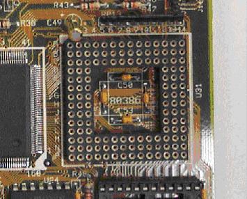
132-pin LIF (Low Insertion Force) socket for 80386 CPU on the motherboard. -
Intel quickly developed an "economy model" of the 386 called the 386SX. The 386SX featured the internal core of the 386DX with full 32-bit registers and instruction set, however it was cut down to a 24-bit address bus like the 286 and a 16-bit data bus like the 286 and packaged like the 286 as well. Since the naufacturing process was greatly improved for superior core speed, the 386SX could be inserted into a 286's socket and run much faster. Since it sold for much less than the 386DX it was a marketing success in that people now had a viable use for the chip as an upgrade to the old 286 CPU on the motherboard. The 386SL would be the first Intel CPU intended for the PC market that would be designed specifically for use in laptops (and other portable PC's.) The SL was further slimmed down in current consumption but is architecturally much more closely a 386DX in that it features the 32-bit registers and instruction set along with the full 32-bit data and address buses. The SL introduces for the first time the SMM interrupt in which the CPU can detect long periods of computing inactivity and then fire the SMM interrupt. If the motherboard is equipped to respond to it, the system can systematically shut down devices thus conserving power. SMM like all other innovations would be carried forward to all subsequent generations of CPU in the x86 family.
-
The 386 would reign for several years while Intel worked on the 80486. This processor was influenced by the emerging very popular new GUI - graphical user interface for DOS called Windows 3.1 and later Windows for Workgroups or Windows 3.11. Because of the enormous processing burden involved in managing and animating graphics on screen in response to user actions at the operating system level (remember that Windows 3.1x is NOT considered an OS instead it is a GUI plug in to one so it does function at the OS level) a much faster and more efficient CPU was going to be needed to rescue users from staring at the hourglass (to wait) most of their computing day. The 486 was Intel's response to the growing need for the horsepower necessary to execute the demanding processing burden of Windows.
-
The 486 features a completely new instruction decoder rebuilt from scratch from the ground up. It is still designed to run the predecessors machine language instruction sets but it decodes them in a brand new way. As as instruction arrives in the instruction decoder it enters the first stage of the decoder which makes a partial decoding interpretation of the instruction. For example (and it is ONLY an example for illustration purposes) the first stage of the decoder may only determine if the instruction is a single byte instruction like the STC instruction which only turns on the Carry flag bit of the Flags register (STC - Set Carry flag) or if it is a multi-byte instruction like MOV AX, [200]. This instruction in binary starts with a byte that means "this is a move of data from a memory location to the onboard AX register" the instruction is followed by the 16-bit (two byte value) 0200 indicating the actual memory address offset that holds the data to be fetched into the register. This stage of the decoder will set an internal flag within the decoder and then pass the instruction forward to the second stage of the decoder. This stage will continue the process of decoding the instruction and pass it forward to the next stage until it is finally completely taken apart and executed. The 486 instruction decoder is five stages deep and is called the instruction decoder pipeline. The instruction decoder itself is a small programmable computer within the computer and it can be reprogrammed in the event that a more efficient microcode can be written to handle the decoding of the actual x86 machine language programs. This microcode can be read from the BIOS during the POST so flashing the BIOS may include CPU microcode changes that greatly improve the function of the CPU itself. Since the pipeline is five stages deep the instruction decoder can actually be working on 5 separate instructions as they move through it at the same time. The instruction decoding efficiency of the 486 is therefore variable depending on the complexity of the program itself but averages between 1 to 2 clock cycles per completed instruction.
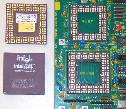
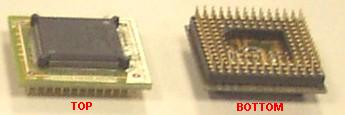
168-pin PGA Intel 80486DX CPU Top and Bottom and a 169-pin Motherboard
Socket (the 4167 socket is for a Weitek Math Coprocessor) -
In contrast the original 8088/86 chips required an average of 12 clock cycles to complete an instruction. The 286 (and the 386) had improved this to about 4.5 clock cycles per instruction. This means that if all else is equal the 486 will run programs roughly 2.25 to 4.5 times faster than the 386. But all things are not equal. The motherboards are up to 33% faster in later 486 models and the processor cores of the 486 are up to 4 times faster.
-
Because of the pipeline decoder the 486 would be the first processor to feature cache memory on board the CPU itself. This L1 - Level 1 cache is only 8KB in size but it is significant because it runs at the speed of the processor core.
-
What makes that significant is that the 486 would be the first processor to feature a clock multiplied core. While the rest of the motherboard and its attachments (RAM, control buses of the chipset, etc) would run at say 33Mhz, the processor itself would run at 66Mhz internally. Since the core has the MMU - Memory Management Unit and the L1 cache it is more likely to have the data that the CPU is looking for than ever before and also at the speed of the core allowing the core to run at full speed without having to execute as many "wait states" awaiting response from a much slower chip on the motherboard. This L1 cache in combination with the clock multiplied core is what makes the 486 up to 4 times faster than the 386 but with the cache and the new pipeline decoder it can effectively perform even faster than that.
-
While Intel was at it they also decided to embed the FPU - floating point unit math coprocessor into the processor core for the first time thus eliminating the need to make motherboards with additional sockets for the FPU and the need to open the system and handle the circuit boards in order to perform the upgrade which of course can lead to the user inadvertantly destroying the system with an ESD. But the story is not yet over, the 486 does have a sordid tale in the midst of its major computer engineering achievements. While conducting the first manufacturing runs of the 486 Intel discovered that they had produced large numbers of chips with faulty FPU's. They corrected the manufacturing die and continued producing fully functional 486's, but decided that they could not simply throw all of the malfunctioning chips away. Instead they reprocessed them disabling the onboard FPU and marketed them as "486SX" chips, 486's without the integral FPU, and the world was none the wiser. Some motherboards for 486SX based systems would be made featuring a "487 FPU socket" Then the user could purchase a "487" and install it on the system and have the FPU's floating point math processing capabilities. The interesting thing about it was that Intel didn't manufacture a "487" FPU although they would market one. The socket and chip were in fact the full blown 80486DX CPU. When installed the motherboard would detect this and simply disable the existing 486 in the other socket and let the "487" be the processor, with FPU, for the system. Someone discovered that one could remove a 486DX from a single socket motherboard and insert a "487" chip into the slot and it would boot right up and work fine ... therefore there was no way that it could be simply an FPU ... it had to be a full blown 486DX which of course it was.
Intel would be involved in a billion dollar lawsuit against AMD - Advanced Micro Devices for stealing their processor core designs and then manufacturing them. AMD would make the cores faster and sell them for less than Intel which really upset them quite badly. They would lose the suit in the U.S. Supreme Court on the grounds that they could not patent or copyright a "part number" Basically they had no product, just a part of a product: the IBM AT. Because of this AMD was free to make the part for the product also. Intel would then name the next processor and apply for trademark on it which would then prohibit AMD and Cyrix from stealing the blueprints and making the CPU. Now they would have to create all new processors that would emulate the next Intel CPU. Intel was sure that the chip was so complex that it could never be done. It slowed AMD down by only a few months and they did successfully emulate the new fifth generation x86 family CPU ... right down to the bugs. This of course was the first PentiumTM processor.
The first Pentiums were actually manufactured on older (possibly designed for making the 80486) equipment and did not feature clock multiplied cores. These chips suffered major cooling problems and most manufacturers did not understand this issue and made their PC's with CPU heat sinks when they desperately needed active cooling fans on the processor. Very few P60 or P66 processor based PC's remain because the CPU's literally burnt up. The common name designation "P60" means "Pentium with a 60Mhz core." Shortly thereafter Intel would start producing the new chip on its own new manufacturing facility and the new VLSI - Very Large Scale Integration manufacturing resolution Intel used was so much better that these subsequent and clock multiplied core Pentiums could run using only a heatsink, yet PC manufacturers had already run into so much trouble from returns while still under warranty that they would no longer risk having to replace a $1000 CPU and started using heatsink/fan assemblies from then on. It would turn out that after the MMX generation of Pentiums, the CPU would always need active cooling systems anyway.
The Pentium generation of CPU introduced a 64-bit data bus. So architecturally it is not a "juiced up" 486 which could be said of the 486 in relation to the 386. That would be technically inaccurate when you inspect all of the engineering changes made in the 486 but a casual nontechnical user could make that claim and be fairly accurate: same registers, same data bus width and same address bus width, just engineers stuff in the core design. However, the Pentium is architecturally different. In fact that 64-bit data bus not only indicates that twice the amount of information can flow across it in either direction meaning that the machine, all else being equal must run twice as fast which is true, those 64 data bus lines feed two instruction decoding pipelines called the "U" and the "V" pipelines. This means that very roughly speaking the Pentium is actually a dual 486 inside.
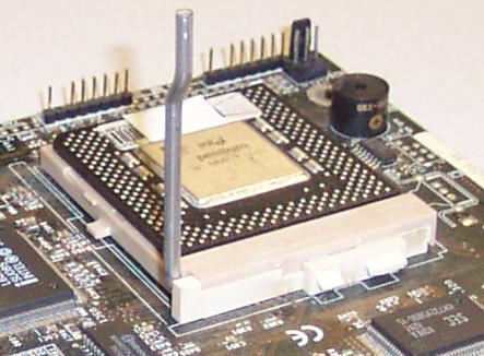
Pentium 5th generation x86 processor in a ZIF - Zero Insertion Force
socket with the latch in the "released" positionThe dual instruction pipelines of the Pentium processor increase the efficiency to the point that the processor has a greater than 1-to-1 instruction per clock cycle ratio. It can literally execute more than one instruction per clock cycle. This is a feature that Intel calls "superscalar execution."
The Pentium core includes two 8KB L1 caches, one for data and the other for machine language instructions that the processor is currently executing. This also greatly improves execution speed since data and program code often reside in totally different locations in main memory.
Each generation of processor brings its own new instructions that are added to the predecessor's instruction set. So the Pentium can execute any and all programs written for the 486 and it can also execute programs compiled specifically for itself. Obviously once a program has been compiled for the Pentium, it cannot be executed on any older processors since those machines will not know what to do when they encounter a Pentium instruction.
The fifth generation CPU's (the Pentiums) would evolve through more technological advances than the entire x86 family before them combined. These will be fully explored in the next class (CET1172C - A+ Hardware Service and Maintenance).
When in doubt the motherboard chipset and motherboard manual will indicate which type of CPUs can be used on the system. In the motherboard manual you should find the possible FSB - front side bus speeds and a mention of the kind(s) and speeds of CPU's that the motherboard will support. Read the manual and find this information and write it down at the end of this module. Notice that there is a front side bus speed selector jumper. Open the case, find the jumper and write down this setting. Based on this jumper and the motherboard manual, indicate what is the front side bus, and what multiplier is needed based on the CPU listed at bootup and what RAM is in use.
Review Questions
-
What was the first microprocessor used by the IBM PC and its clock speed and average number of clock cycles per instruction?
-
What was the microprocessor introduced in the IBM AT and its number of clock cycles per instruction?
-
What was the first CPU to feature protected mode? How much RAM could it address? What was the main problem with this processor's protected mode that was fixed in later models?
-
Describe protected mode and multitasking both cooperative and preemptive:
-
What was the first full 32-bit CPU for the IBM PC industry? What manufacturing process/materials were used to make it?
-
Describe the difference(s) between the 386DX and the 386SX processors:
-
What was the first CPU to feature a cache MMU onboard, why was this moved onboard the CPU?
-
What was the first processor designed specifically for laptops nad portable PC's and what new technology did this processor introduce?
-
What was the first CPU to feature onboard cache and how many blocks of cache does it have and what was its size?
-
What was the first processor to feature a clock multiplied core and what were the three most common chips (multipliers) available and define their motherboard front-side bus speeds, multipliers and core speeds?
-
What was the first CPU to feature a "pipeline" decoder, how "deep" is it and describe how it works?
-
What was the first CPU to feature an integral FPU?
-
Describe the difference(s) between the 486DX and the 486SX:
-
What was the first processor to feature more than one block of onboard cache, how many blocks did it have and what was their capacity?
-
What was the first processor to feature multiple "pipeline" decoders? How many did it have? What are their names?
-
What was the first processor to feature a full 16-bit wide data bus? What computer did it first appear on?
-
What was the first processor capable of addressing or supporting up to 4GB of RAM? What commonly listed CPU feature determines this capability?
-
What was the first processor to feature a 64-bit data bus?
-
What is superscalar execution? What was the first processor capable of it and what makes it capable of it?
-
What new technology was included in the P55 series of chips over the P54's, how many instructions are in this technology's instruction set and what does it facilitate?
-
Despite the answer to #51, what really made the P55 so much better? describe it in detail.
-
What was the first sixth generation processor produced by Intel? What is the most obvious difference between a P6 and a P5?
-
What was the first processor to feature a sizable core speed L2 cache? What were the three sizes available?
-
What was the codename and the common (marketing) name for the first mass produced P6 and what were the main differences between it and the very first P6 models?
-
Two variants of the CPU in #55 were made. An economy model and a very powerful server model. List these variant's marketing names and the differences between them and the "regular" version of the CPU.
-
Give the codename and common name for the processor that introduced SSE? What does this stand for and what does the acronym within this acronym stand for? Describe these technologies and how many instructions are in SSE.
-
Other than SSE, the processor in #57 was no major technological advance over its predecessor until it was produced using the new 0.18µ manufacturing process. What was the codename of this chip and why was this manufacturing process so important and worth waiting for?
-
Describe the Willamette. Give its marketing name, rough speed ranges, cache's, and any other unique features that it introduced.
-
Describe the Merced. Give its marketing name, rough speed ranges, cache's, and any other unique features that it introduced.
-
Give one reason and the main operational difference between the AMD Athlon64 and the Intel 64-bit processor which might be reason enough to take the AMD over the Intel chip. (even if all else including core speed, throughput, cost, etc were equal)
-
Name the three main types of register discussed in this lesson and name an example of each:
-
The CPU will fetch the next machine language program instruction based on the values stored in which air of registers?
-
Despite the fact that all of the 8088’s registers are 16-bit, explain how it generates a 20-bit physical RAM address from cs:ip register pair assuming that the cs = 1230h and the ip = 0045h:
-
The stack is a special section of memory that functions as what kind of buffer?
-
The stack has a default function within many instructions including, for example, a long jump to a subroutine in another code segment of RAM. Explain what the CPU does using the stack in order to find its way back from the distant subroutine.
-
Name the three default segment registers and what they point to in RAM for the average program:
-
Describe the function of the memrw line.
-
The 8088 basically is a computer designed to operate on numbers stored where?
-
Basically all the 8088 does is _________________ , _________________ , and _________________ machine language instructions stored in RAM.
-
The number on the address bus specifies the actual specific location in ___________ that the machine is either reading in or writing out to.
-
The binary number placed on the address bus is decoded by what type of circuit in order to activate the unique memory cell that it represents?
-
The individual RAM address ______________ circuit is the one that inspects the state of the memrw
line from the CPU. If it is in the "read" state, this circuit will place the contents of the individual bit cells
of this memory location onto the ______________ bus and if it is in the "write" state this circuit will
______________ the values on the data bus into the individual bit cells. -
Go to http://www.intel.com and search their site for this CPU type and gather as much information about it as possible. Are there any known “errata” (bugs)? Are there any support downloads for the processor? Print or save the web pages for future reference.
-
For homework find out what processor and type and speed of memory your own personal computer is using. You do not have to open the case to find out, find the documentation for the system that it came with or go to the manufacturer's website and look it up. if you have a custom built machine determine the motherboard/BIOS serial numbers during boot up and try to find its documentation online. On a custom built system you may have to open the case and inspect the motherboard to find the manufacturer and model number in order to find the documentation online. Also try to determine again using the online documentation the processor and type of RAM in your computer at work (if you have one) or even a friend's PC, or the one at your nearest public library, etc.
-
Main Startup BIOS screen information:
Processor type:
Processor Speed:
Amount of RAM:
BIOS Serial Number:
BIOS Mfg. Name:
Motherboard Mfg:
Additional Info:
-
Information from the Manual and Windows Utilities:
Processor manufacturer:
Processor Model (Name):
Processor Core Speed:
Processor L1 Cache(Amt):
Processor L2 Cache(Amt/Speed):
Processor Core Multiplier:
FrontSide Bus Speed(Core/Mul):
RAM type/amt/speed/thru-put:
Additional Notes:
-
Processors:
| Name | Codename(or #) | Regs | Addr | Data | Notes: |
| 8088 | 8088 | ||||
| 286 | 80286 | ||||
| 386 | 386DX | ||||
| | 386SX | ||||
| | 386SL | ||||
| 486 | 486DX | ||||
| | 486SX | ||||
| Pentium | P5 |
Copyright©2000-2007 Brian Robinson ALL RIGHTS RESERVED