CET1171 Lecture #8 - Memory Technologies
Materials: Working complete PCStudent bootable floppy diskette - "New Boot A Version 2"Student bootable CD-ROM Working complete PCStudent bootable floppy diskette - "New Boot A Version 2"Student bootable CD-ROMObjectives: List and describe the various memory technologies including,Each memory's features and capabilities,Each memory's limitations,Each memory technology's most common usage,Be able to identify which memory is installed in a system,Know the RAM associated with each generation of CPU.Competency: The student will be able to describe all major generations of memory technologies of the IBM PC and be able to determine which type of memory is installed in the system. The student will be able to identify the RAM technology requirements for the system and be able to run diagnostics for the CPU, and RAM. |
-
Boot up the PC. Due to the large number of PCI devices in the device listing of the text mode BIOS screen the CPU type always scrolls out of view. This will probably be the norm on late model PCs. Enter the BIOS and disable the Quick Power On Self Test feature. When you reboot the BIOS will perform a memory count. During this phase hit the Pause/Break key. Now record the processor type, total amount of memory and type if indicated, and the BIOS serial number across the bottom of the screen. Use the serial number on the web to determine if the system already has the latest BIOS update by investigating this online.
-
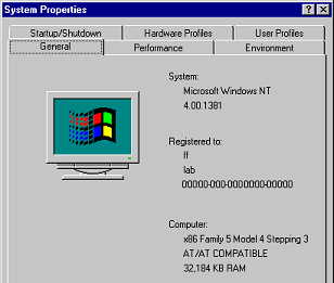
Start Windows in Normal mode and Right click on My Computer and select properties. Make a note of the processor and RAM reported. This only reports RAM amount but not the type. Under this 'General" tab of the system properties sheets the processor is also listed. In the case of later versions of Windows and Intel CPU's the family and steppings are indicated. Record these values then go to the Microsoft and Intel websites and determine the processor based on this information.
-
The student must learn the various types and categories of RAM. There are many different ways to categorize RAM: the physical package, or the appearance and form factor of the RAM memory components that can be installed on the PC, and the electronic RAM technology, or the manufacture and design of the RAM at the circuit component level which differentiates between successively faster generations of RAM, to name just two.
-
There are three major classes of “random access” memory circuits found in the modern digital electronic computer of which the PC is no exception: DRAM - Dynamic Random Access Memory, SRAM - Static Random Access Memory and ROM – Read-Only Memory. ROM's are special RAM circuits that do not lose their data when the system board loses power. ROM technologies, covered in Lab #9, are used to hold the BIOS. This lecture describes DRAM and SRAM. Both of these lose their data when the chips lose power. This is called volatile memory. NVRAM – Non-Volatile Random Access Memory is a term often used to refer to the CMOS RAM to differentiate it from ROM and normal RAM.
-
Dynamic RAM is the basic form of RAM that the PC uses and which is the one referred to when users proclaim: “My computer has 512MB of RAM.” Dynamic RAM is far less expensive than static RAM because each bit cell of storage within it requires a circuit consisting of one transistor and one capacitor.
-
When data, either a “1” or a “0” are placed into the cell, the capacitor charges up and then slowly bleeds off into the transistor thereby keeping this switch set to the correct value. But a microscopic capacitor’s voltages and amperes of current are extremely small, so the capacitor can only hold the transistor in the correct state representing a “1” or a “0” for a small fraction of a second before it bleeds out all of its electricity holding the value.
-
Therefore refresh circuitry must continuously strobe through every memory location recharging the bit cell capacitors so that they do not lose the value that they are holding and providing to the transistor of the bit cell. The refresh circuitry constantly strobes through all of memory refreshing the cells so that data will not be lost. This one transistor plus one capacitor circuit that must be actively refreshed at regular periodic intervals is the definition of dynamic RAM.
-
Static RAM on the other hand has a circuit made up of six transistors for each bit cell. These transistors in essence switch each other on or off and thereby hold the state of the circuit, as a whole, stable without needing the capacitor. Because these transistors form a stable switching circuit for either state, holding voltage or not holding voltage at the proper point in the circuit, they do not require constant refreshing like the dynamic RAM bit cells do.
-
This has several effects on the bit cells. One, they can switch into another state at the reactivity speed of the transistors themselves which is always quite fast compared to other types of circuit component, especially capacitors. In comparison a dynamic RAM bit cell can only switch states at the reactivity speed of the capacitor which must either charge up and in doing so collect current to represent the "1" for example, or it must discharge the current it is holding so that it can represent the "0", both of these actions take far longer than the switching speed of a transistor. In the earliest RAM circuitry used in the PC, the dynamic RAM bit cells had an access speed of 200 nanoseconds or 200 billionths of a second which certainly does not sound like an eternity, and was entirely the result of the longer reactivity of the capacitors in each bit cell. In contrast, the average single transistor of that time had a reactivity time of about 4 ns. So a static RAM bit cell containing a total of six transistors would at worst take about 30 ns to change state. In comparison, the DRAM cells did in fact take an eternity to react to a change in data they were holding.
-
The second effect of pure transistor static RAM bit cells is that they do not require refresh circuitry at all. This means that any time the CPU makes a read/write request to a static RAM address it will always be available. This is not the case with dynamic RAM. The CPU might make a request to the dynamic RAM address at the same time that the row or column of addresses is being refreshed. In that case the CPU will be sent “wait states” until the refresh circuit is done and moves on to the next section of the RAM address array, then the data can be accessed and delivered to the processor. This obviously slows down the overall performance of the computer.
-
Third, because static RAM chips require a minimum of six transistors per bit cell while dynamic RAM chips require a minimum of one transistor and one capacitor for a total of two components per bit cell, then all other things being equal (the size of the silicon wafer, quality, etc) static RAM must be at least three times more expensive per bit to manufacture. Often because of the extreme speed, superior manufacturing materials and methods are used leading to even higher costs.
-
Because of the high price of static RAM compared to dynamic RAM even when counting the entire dynamic RAM refresh circuitry, DRAM is so much cheaper that it has always been used in personal computers. The IBM PC has been no exception, but static RAM has been used in limited quantities the PC in the form of cache which has greatly improved performance without greatly increasing the price.
-
Cache in the PC industry refers to a temporary fast memory storage intermediary for any main storage technology that is slower than the cache. The slowest storage devices today are the floppy disk drives and the optical drives (CD-ROM readers and burners and DVD-ROM readers and burners) although these are improving enormously by their usage of cache memory.
-
One of the main reasons that the HDD has become so fast lately (UDMA133 and SATA-150) is that the drive has built into it a large RAM memory chip usually greater than 2MB in capacity that it uses as cache. As the drive seeks the file that the operating system has requested, when it hits the correct track and head it will read the entire track into its onboard cache, if more data is required from another location, the drive will find the requested data within the cache and begin transmitting it to the system while it seeks the new track/head location, as it finds the data, the drive reads this whole track up into the cache again. This behavior will continue such that the drive does not have to be as accurate during read operations, the electronics (much faster than the drive heads) can sift through the track read and locate the actual sectors that were requested and begin transmitting the data while the heads reposition over the next track. This usage of cache means that the data flow will proceed with far fewer interruptions. Drives only bog down when massive read/write operations are occurring or when a video stream or other huge file is being read.
-
This leads to the next level of cache. DOS employed SMARTDRV.EXE in a role similar to what the VCACHE occupies in the Windows OS kernel: a read/write cache buffer implemented at the software level. This disk caching is managed by the OS utility, the HDD and the ATA controller are not involved in that they do not possess the memory (it is regular system RAM) nor the algorithm (program) that is performing the operation. SMARTDRV and the VCACHE are designed to anticipate future read/write requests of the HDD. They literally run a program that attempts to predict what information might be requested next from the HDD. When they figure a likely future read request they make the request during any idle moment before it has actually been requested by the OS or the user and read the HDD data into a large section of RAM set aside for this. If successful, when the system does finally actually make the request, the data has already been placed into the RAM disk cache and will be delivered from there thousands of times faster than it would if it has to be physically cahsed down from the surface of the HDD platters.
-
The average user has seen this behavior in Windows anytime a program is run, then closed, then run again. The second time the program opens much faster. Part of the disk caching algorithm bets that if the user ran a program once, there is a good likelihood that the user will run it again so it keeps it in RAM cache just in case.
-
Of course cache prediction cannot be perfect. If it were I would certainly start to worry about a program that can anticipate every single thing I do on my PC! So the job of the programmers is to design cache algorithms that are efficient. That is, they have a good hit to miss ratio but do not consume so much processor time and system resources that it would slow down the overall performance of the computer.
-
The processors have also had cache built in to them since the 486. This is implemented at the hardware level meaning that the chip itself has hardwired into it the program and the circuits called the MMU - Memory Management Unit, that will make predictions about the future main memory locations containing program code and data that the actual processing section of the chip will need next. The cache management section of the chip will make these predictions and prefetch main memory information into the cache memory locations which are much faster than main RAM. If the chip does in fact need the data then it can continue executing at close to core speed with no delays. If the processor needs program code or data that the cache manager did not anticipate, called a cache miss, then it must make the requests from main RAM memory which runs much slower, at front side bus speed, or worse if the RAM is slower than that, rather than core speed.
-
The cache in the Pentium generation chips have been split into two independent levels: L1 and L2. The Pentium has two relatively small L1 (8KB originally and later 16KB for the Pentium MMX and later) caches; one for data and one for program code. These have their own prediction program and prefetching circuitry and are onboard the actual processor chip itself and always run at full core speed. They fill themselves out of the high speed L2 cache whenever possible. This is in fact how the L1 can even perform fast prefetches at all, because it fetches from L2 which is also faster than main RAM. The L2 operates independently of L1 but is run by the same cache memory management unit(s) on the CPU. By independently it is meant that the cache manager also inspects the current program and makes predictions about what will be needed in the future but it uses a different prediction algorithm and makes larger RAM block prefetches which come from the slow main memory when deciding what to pull forward into the L2 cache. Pentiums can manage up to 512KB of L2 cache which was static RAM on the motherboard up to the Pentium II's and partial or full core speed onboard the CPU thereafter, either of which is faster than regular dynamic RAM. This is where static RAM has been used in the PC with great success in terms of performance improvement without having to invest large amounts of money on it.
-
It is this ability to efficiently predict future data and code requirements of the CPU such that the information can be prefetched into high speed, even core speed, memory before the chip actually requests it, that make the Pentium generations of CPU appear so fast. On occasion AMD, and even Cyrix, makes a break through in cache technology (the prediction algorithm, and/or the organization of the cache memory) that makes it so much more efficient that their chips appear much faster when the manufacturing process has not changed at all. This is what happened with the Cyrix MI and MII chips as well as some of the AMD Athlons.
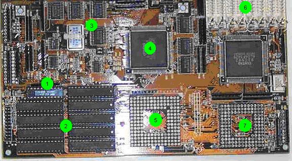
Components Indicated
- Tag RAM chip, used to hold the memory translation organization (what addresses the cache will respond to)
- SRAM cache chips, DIP packaged in sockets
- Quartz crystal, provides oscillations that drive the motherboard front side bus clock generator circuits.
- Motherboard chipset (the other large chip above the FPU socket also)
- Processor LIF – Low Insertion Force, socket for 386 CPU.
- 30-pin SIMM slots, two banks or four slots each.
- LIF socket for the 80387 FPU – Floating Point Unit (math coprocessor).
-
In the original PC RAM was purchased as individual IC – Integrated Circuit, chips that could be inserted individually into standard IC sockets soldered directly to the motherboard. This was the standard packaging of the day for these digital components and such an IC is called a DIP – Dual Inline Pin, package. Rows of empty DIP sockets were soldered to the original PC’s motherboard that could accommodate the maximum amount of RAM that the system could accept. The system would then have installed into the sockets the amount of RAM that the user chose to purchase. Conventional inexpensive electronic DIP RAM chips were made in 14, 16, or 18-pin varieties, but other standard DIP sizes do exist.
-
At a later time if the user chose to upgrade to more memory, then a technician could install the RAM IC’s onto the motherboard totaling the amount of RAM that the user desired. The generic RAM chips are not always arranged in byte sized address locations. Often they have anywhere from one, two, four, or eight bit cells at each address. And their internal array may have anywhere from 2048 (2K), 4K, 8K, etc, of addresses. This meant that the correct types of chips had to be installed into the correct sockets in order for the motherboard demultiplexing circuitry to recognize complete 8-bit wide addresses of RAM.
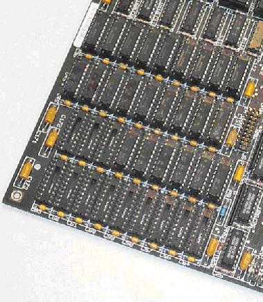
AT motherboard equipped with DIP
packaged RAM showing empty DIP sockets -
While these are electronics industry standard components, they do not actually work well in DIP sockets for two reasons. One, they are rather difficult to insert and remove and can easily be damaged in the process. And two, because the of the fact that the CPU is executing program code that is scattered throughout these chips, at any given time the CPU is actively reading and writing to one area of program addresses that physically reside within a few of these chips and so they heat up from the activity, but then the program jumps to another location in memory and the CPU begins heavy read/write activity at those addresses which physically reside in several other chips, so these begin to heat up from the activity while the others cool off. Then the CPU jumps to another set of addresses, causing those chips to heat up and the others to cool off.
-
This constant heating and cooling of the individual RAM chips causes the phenomenon called “chip creep.” Over time, the chips will work their way out of the sockets until they are so loose that a pin or two no longer make contact with the hole in the socket and the chip fails with memory address errors which crash the program and the entire session must be aborted and the system must be rebooted. But the address will be hit again, so the system will not work until the chip is reseated.
-
This meant that the PC had to taken to a technician who would simply press all of the socket mounted chips down firmly into their sockets with his thumbs taking but a few minutes, but charging quite a bit of money for the visit. And chip creep could under heavy use loosen chips within a month or two and it was a nuisance in time lost taking the system in for repair and in the cost of the technician.
-
The situation would inspire change. IBM would develop a small circuit board card to which the individual chips were soldered. The card itself had a long row of pins along one edge and could be pressed down into a special slot made of pin socket holes that was soldered to the motherboard. This first specially designed memory expansion module for the PC was called the SIP – Single Inline Pin, package. They are also sometimes called SIPP, the second “P” is for the word “package.”
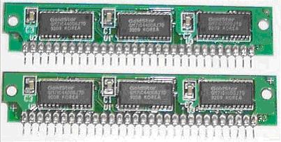
Original industry standard 30-pin SIPP -
SIP modules solved the problem of chip creep because the constantly heating and cooling RAM chips were soldered directly to the small circuit board which could dissipate heat much better that the direct metal contact of the pins and the socket holes themselves. However, they did not solve the problem of the very fine pins themselves that can easily be bent and broken especially while trying to remove the module. Another problem with SIP modules is that they stand up on the row of weak thin pins and if they are even mildly brushed against they will bend over bending all of the pins. The natural reaction is to bend the module so that it stands straight again. And what happens when metal is bent back and forth? Yes, it is almost a guarantee that at least one of the fine little pins will break when this happens. Or it will break the next time it happens when the case is opened.
-
Seeing this, IBM changed the RAM module design again, this time instead of actual pins of metal sticking out the side, the pins are actually small metal squares on the edge of the circuit board card. The card is then pressed into a slot with contacts that meet up with these. While they were at it they made a latch/release mechanism on the slot to securely hold the module so that it would not be brushed over like the old SIP. The snapping action of the latch clips also physically indicated that the RAM module was properly installed.
-
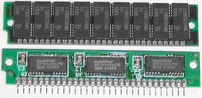
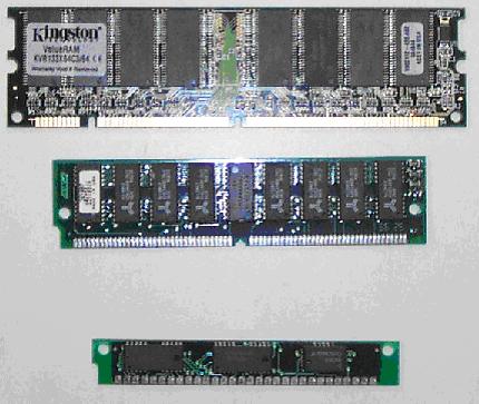
A RAM module with the edge connector pins is called a SIMM – Single Inline Memory Module. The first ones were made to replace the SIP packages and had the same bus and support line wiring. These had 30-pins and a data bus that was 8-bits wide. The most commonly seen capacities were 256KB, 512KB, 1MB. 4MB modules were also made and were the largest possible that could use the address bus pins available. Larger 30-pin SIMMs are possible but they would have to use other pins for addressing and would probably only work on proprietary motherboards designed for them.
-
RAM modules are always manufactured in exact even binary multiples in capacity because of the fact that they hold exactly the number of address cells as they have active address bus lines. This means that if a module has 20 active lines, then it can demultiplex a 20 bit number. 220 = 1,048,576. Since each address holds one byte, then such a module could hold 1MB and it would be referred to as a 1MB module. The next largest module would be able to decode a 21 bit number, so 221 = 2,097,152 bytes or exactly 2MB. Add another bit to the address bus and it will double the number of addresses and therefore bytes of storage yielding a 4MB module. This is why 3MB RAM modules and other such in between numbers are never made.
Original industry standard 30-pin SIMM (top)
Compared with a standard 30-pin SIPP (bottom) -
These memory modules were extremely popular since they solved the original problem of chip creep and the problem of casually brushing into them and destroying them. They had become and industry standard by the time the 386 CPU was released.
-
However, the 386 CPU has a 32-bit wide data bus. Therefore, each time it makes a memory request, it wants a 32-bit wide response, not an 8-bit response, which is the data bus width of the 30-pin SIMM. This meant, that on systems equipped with the “real” 386 (the 80386DX) that four 30-pin SIMMs had to be installed into the four slots that were wired so that the motherboard would address them in such a way that each could send back its 8-bit wide slice of the 32-bit wide memory request. This group of SIMMs form a memory bank of the processor.
-
Many end users realized how easily these modules could be handled and so they bought their RAM modules and took them home to install themselves. What they did not realize was that they had to buy four matching SIMMs in order to complete a single addressable memory bank and they rarely bought this many since they were still rather expensive. (About $100 for one 1MB SIMM, who was going to buy four at one time?)
-
Of course the single SIMM did not work and so they brought it back for a refund. And of course the end users are not electronic technicians and most likely did not handle the RAM module using proper ESD precautions so many more than one might imagine had been destroyed from improper handling anyway.
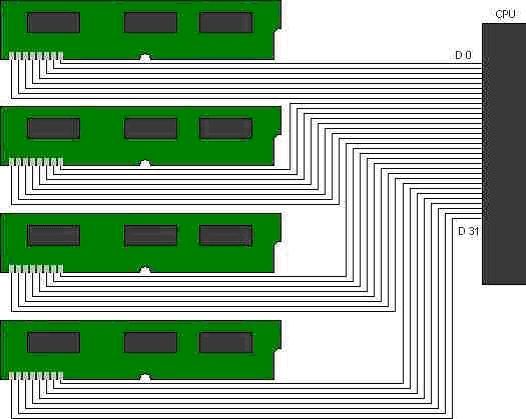
Four industry standard 30-pin SIMM's each 8-bits wide are
Attached in parallel to complete a single 32-bit CPU memory bank -
Since the manufacturers had to absorb these losses while honoring a fairly standard “90 day return if defective” policy, they decided to rectify this situation. From the 386 forward the processors were going to be 32-bit CPUs. This prompted IBM to create a 32-bit wide SIMM module so that one module would complete a memory bank for the 32-bit processors. This way, if the user bought one SIMM and installed it, then it would work and they would not handle it a second time doubling the probability of damaging it. These new SIMMs had to be larger and had to have a higher pin count, their data bus width of 32-bits by itself was wider than the entire edge connector of the 30-pin SIMM. The new SIMM was 72-pins wide and were available in sizes from about 2MB to 32MB. Larger ones were made but these probably only worked on proprietary motherboards for which they were specifically made.
-
Both types of SIMM have a notch on one side to prevent them from fitting properly if inserted into the SIMM slot backwards. Both types must be inserted into the slot at a 45° angle and then they are rocked into position which forces them into the latch clasps that snap past the edge of the module circuit board edges and hold it firmly in place.
-
During the time of the SIMM, from the introduction of the IBM AT in 1985 up through the 486 in the early 1990’s, motherboard chipsets and the SIMM RAM modules were designed to support two different types of data set: raw, which is the type of data one imagines in which each address holds the 8 bits of the byte. The other data set type of RAM is called parity.
-
Parity RAM holds the original 8 bits of the byte within the address location, but it also adds another extra bit, the parity bit as well. So each address is actually composed of a total of nine bit cells instead of the plain eight bit cells at each address of plain or non-parity memory.
-
Parity is a form of error detection code. It enables the motherboard circuitry to determine if the data being retrieved from that memory location has been corrupted. If so it can then act accordingly. There are two forms of parity: even and odd.
-
In odd parity, for example, the total number of ones within the byte must be kept an odd number. For example:
 Original Byte
  0 1 1 0 1 0 0 1
 has 4 ones in it, an even number of them so it will be stored in the
 parity RAM location which has NINE bit cells as:
  0 1 1 0 1 0 0 1 1 <=Parity bit forces total number of ones to be odd
 Now this address has a total of 5 ones which is an odd number of them.
 If the byte: 01110000 is then stored it will be stored in the nine bit
 cells of its address as:
  0 1 1 1 0 0 0 0 1 <=Parity bit keeps total number of ones odd
 Now this address has a total of 3 ones which is an odd number of them.
-
So the parity bit can always force the nine bit location to have an odd number of ones regardless of the value of the original byte to be stored in it. Even parity works exactly the same way except that it keeps the total number of ones in the nine bit cells of each address an even number of them instead of an odd number of them.
-
Now if any bit amidst the nine bits within an address gets changed accidentally, then the total number of ones will no longer match the parity type. For odd parity if the values in the bit cells are:
0 1 1 0 1 0 0 1 1 <= Parity bit of 1 And if bit #3 changes from a one to a zero like this: 0 1 1 0 0 0 0 1 1 <= Parity bit of 1 Then the total number of ones in the nine bit cells of this address is now 4, an even number which is not allowed. -
The motherboard circuitry will detect this and then the error can be acted upon. Most SIMM's were not interchangeable. If the motherboard needed parity RAM, then parity SIMM's had to be installed in which each address consisted of nine bit cells instead of eight. If the motherboard needed non-parity RAM then non-parity SIMM's had to be installed on it. A few late 486 model motherboards could either be configured with jumpers or BIOS settings or even automatically detect which type was installed and then adjust the dynamic RAM controller circuitry to use which ever type was installed. But for the most part motherboards would absolutely refuse the wrong data set type of RAM.
-
While parity sounds like a good idea its implementation in the PC was to be blunt, horrific. Since the hardware circuitry in the motherboard chipset is the one detecting the error, it handles the error at the hardware level as well. That is, the machine would activate the non-maskable interrupt, or NMI of the CPU. Like its name sounds, this interrupt cannot be masked or disabled, the CPU will respond to it, and since no operating system had a handler for it, the BIOS handler would indicate that a parity error had occurred at a particular address and then lock up the machine and force a reboot. An extremely unpleasant event while in the middle of typing a very large paper and losing all of it rather than a single byte of it which is what the parity error detected.
-
This nasty event became extremely unpopular such that end users vehemently insisted on verifying that the PC they were buying did NOT have parity memory in it. They did not care about anything else, “just show me in the specifications that this machine does NOT have parity.” The consumers would speak again. Parity would quickly disappear from the PC.
-
But the removal of parity subsystems in the RAM controller circuits only gets rid of that terrible complete halt when a parity error occurs, but it certainly does not end the fact that on occasion single bit errors do occur. Knowing how the CPU works, it is obvious that the change of a single random bit in RAM will change a machine language instruction which will crash the program immediately. What causes these errors? How common are they? And what can be done about them?
-
The question of what causes these random single bit memory errors was indeed a mystery. As far as some of the leading computer engineering experts could tell, there were three main causes:
- Poor quality components, especially power supplies with cheap parts that lead to excessive “ripple,” the subtle leakage of the original wall AC 60Hz oscillation into the converted DC voltages on the internal circuitry side of the power supply. These can never be completely eliminated unless active voltage regulator circuits are used which make the manufacture of the power supply more expensive and also increase the waste heat generated within the power supply. This means that extra heat sinks and better fans would be required further increasing the cost of the power supply.
- Radioactive decay within the materials out of which the RAM chips are manufactured. Almost all materials on earth have a very small quantity of radioactive matter within them, the silicon wafers out of which the chips are made are no exception. The amount is so small that it has practically no effect in most ordinary items, but in the miniscule transistors of RAM chips a single atom’s radioactive decay releases enough energy sometimes to change a zero into a one.
- Cosmic Rays from outer space. Actually, true cosmic rays never reach the surface of the earth, or life could not exist on earth. However, cosmic rays impact with the atoms of the ionosphere (through which the shuttle orbits) and are converted into other high intensity forms of radiation. These in turn collide with atoms in the upper atmosphere and are converted again. These rays collide with atoms in the lower layers of the atmosphere and are converted into “tertiary cosmic rays” which are simply free high speed electrons. These seem to be tolerable to the lifeforms on earth, but they can and do cause rare damage to cells including cancer, and genetic mutations (at a rate of less than 1 in 10,000). But they are also numerous enough that they can and do cause random single bit corruption within RAM chips.
-
The PC industry has done what it can with the first two causes. Power supplies and the general quality of all components has steadily and markedly improved. The materials out of which RAM chips are manufactured are of a much higher quality with reduced radioactive impurities. But only lead cases could stop tertiary cosmic rays, although in fairness only an extremely small number of tertiary cosmic rays actually reach the inside of the PC’s metal enclosure where it sits inside of a building.
-
However, the amount of program occupied RAM is growing steadily. In 1981, the DOS kernel may not have occupied a full 100KB of RAM. Windows 95 needed 4MB in order to load and run (miserably slowly). Windows XP needs at least 128MB of RAM to load and run miserably slowly and there is no end in sight of this run away explosion in program size. The more RAM is in use, the more likely a single bit corruption will actually occur within the occupied area which will lead to a crash. And with each passing generation of RAM technologies, the individual transistors within the chips are getting smaller and smaller, meaning they are getting more and more vulnerable to a nearby radioactive event.
-
While the quality of materials and the quality of circuit design has improved, it has not completely eliminated these factors from damaging information in RAM. In order to prevent such crashes from occurring in mission critical applications including network servers, another type of RAM has been developed, one that uses an ECC – Error Correction Code, data set.
-
While parity is an EDC – Error Detection Code, technology that adds the cost of a single extra bit cell to each byte’s address of RAM, ECC - Error Correction Code adds quite a few more bit cells to grids of addresses, but instead of just detecting the error, it can also correct it on the fly so that the system never receives erroneous data from RAM. (Within the limits of the ECC algorithm, single bit errors are always correctable, but multiple bit errors may not be. But these are far more rare than single bit errors.)
-
The algorithms (formula designs) actually used in ECC are quite complex, in fact there is a whole branch of computer engineering and computer science devoted to developing more powerful ECC algorithms, I have devised a rather simple and horribly inefficient one called the Robinson ECC Algorithm to demonstrate that ECC is possible and how it fundamentally works.
-
Imagine that the sample machine uses 4 bit memory locations instead of 8 bit byte sized locations like the PC. And the algorithm uses 4 neighboring memory addresses. Here is an example of the four neighboring four bit addresses and their contents:
  0 1 1 1
  1 0 1 0
  1 0 0 0
  0 0 1 1
-
Now imagine that an odd parity bit will be stored for each four bit address:
  0 1 1 1     0
  1 0 1 0     1
  1 0 0 0     0
  0 0 1 1     1
-
Also imagine that another odd parity bit will be calculated for each column of bits through the block of data bytes:
  0 1 1 1     0
  1 0 1 0     1
  1 0 0 0     0
  0 0 1 1     1

  1 0 0 1
-
Now if any single bit within the original stored data matrix gets damaged, its location can be pinpointed. If the location of the damaged bit can be determined, then the circuit can switch it back to the original value again, retry the parity calculations to verify that the correction works and then pass the information on to the requesting circuitry:
0 1 1 1 0<=CORRECT, total ones are odd 1 0 1 0 1<=CORRECT, total ones are odd 1 0 0 1 0<=INCORRECT, total ones are even 0 0 1 1 1<=CORRECT, total ones are odd 1 0 0 1 ^ ^ ^ ^ | | | | | | | +-----INCORRECT, total ones are even | | +-------CORRECT, total ones are odd | +---------CORRECT, total ones are odd +-----------CORRECT, total ones are odd -
Since the system can detect which row and which column the parity errors are on, then the intersection of these must be the problem bit. The system would change it to the opposite of whatever it is (from a “1” back to a “0”) and then recalculate the parity for the entire grid. All parity bits would be correct and then any one or all of the four addresses data could be delivered to the data bus.
-
All ECC works on variations of this basic concept but they are much more efficient. Most RAM ECC is capable of correcting a single bit error which is by far the most common, but cannot correct multiple bit damage, in that case the system will just have to go ahead and crash and be rebooted. But since random single error damage is probably common enough to occur perhaps once a month on very busy network servers running enormous operating systems and applications and handling many gigabytes of traffic per hour, then it prevents these crashes and stabilizes the machine noticeably. Multiple bit damage would probably occur at a frequency of probably once per decade on the same system. This would be an acceptable rate of crashing due to random bit errors on even critical machines. (That is, the occurrence of crashes can never be deduced to never.)
-
In the meantime, two significant electronic memory technologies would be developed for the SIMM memory modules. 30-pin SIMM's were comprised of electronic industry standard DRAM chips made using a standard TTL - Transistor-Transistor Logic manufacturing process. These standard DRAM chips probably averaged 150ns to 120ns access times. The original DIP, the SIPP and the 30-pin SIMM are associated with TTL. During the operational lifespan of the 72-pin SIMMs which spanned the 386, 486 and early Pentiums, the need for faster RAM to keep up with the rising speed not only of the CPU itself but also the motherboard chipset components and front side bus put pressure on the memory manufacturers to develop their own high speed RAM chips. The first of these was referred to as FPM - Fast Page Mode, RAM.
-
FPM RAM takes advantage of the actual memory cell demultiplexing circuit process. The demultiplexers within the RAM chip, decode the binary address on the address bus into the row and column location of the eight bit cells that hold the byte of data of the address, and then activate those selectors to either read or write to the specific location within the memory array. Engineers found that they could hold the row selector line within the chip “on” between address requests. If they did this, then only the column selector had to be demultplexed in the subsequent address request. This would eliminate at least one clock cycle delay in demultiplexing the row selector within the RAM chip itself during a memory read/write operation but it would only work if the next address request was on the same row of memory addresses as they are arranged internally within the chip. But it was a start.
-
A superior redesign of this principle would appear in RAM chips called EDO – Extended Data Out. These organize the rows and columns and demultiplex these selectors more efficiently and again hold the row selector line “on” between address requests and can achieve “zero wait state” memory read/writes to subsequent binary addresses until the end of the row of their arrangement within the chip.
-
EDO is the most efficient form of basic DRAM widely used in the PC industry and averaged an access time of 60ns. 72-pin SIMM packages are often associated with this electronic memory technology. Old DRAM 72-pin SIMMs probably averaged between 120ns to 90ns prior to the development of FPM and EDO types.
-
The Pentium processor introduced a 64-bit wide data bus. Because of this the situation returned that had existed in the 30-pin SIMM era, two matching 72-pin SIMMs were needed to be able to respond to a single memory read/write request. This is because 72-pin SIMMs have a 32-bit wide data bus. Users and even technicians did not know why, but they quickly learned that a Pentium based system had to have SIMMs added to it in matching pairs.
-
The memory module manufacturers had already learned what this would mean from the old 30-pin SIMM problems of requiring more than one module in the correct slots in order to complete a memory bank. A new standard physical memory module package was quickly developed: the DIMM – Dual Inline Memory Module. This module has the circuitry of two SIMMs on a single RAM expansion card, hence the name. A DIMM module has 168 pins but unlike the SIMM which has a single row of 72 pins across the bottom, the DIMM has a row of 84 pins on each side of the bottom edge. DIMMs are inserted vertically straight down with even pressure and latches on each end swing up into notches on the sides to secure the module. These are pulled out and down to release the module. DIMM’s have a 64-bit wide data bus to accommodate the Pentium so one fills a Pentium memory bank.
-
DIMMs were developed based on EDO RAM chips, but a superior electronic RAM technology would soon emerge that would instantly render EDO obsolete: SDRAM – Synchronous Dynamic Random Access Memory.
-
SDRAM is based on the concept of synchronizing (hence the name) the refresh circuitry operation with the CPU operation clock cycles. That is, during the front side bus clock cycle which the CPU multiplies into the core frequency, there is a narrow “window of opportunity” in which the address bus will actually bring an address request to the RAM chips. The rest of the time, the address bus will not bring an address request to the chips because the CPU is doing other things at that time like decoding an instruction internally.
168-pin 64-bit SDRAM DIMM (top) compared with
72-pin 32-bit SIMM (middle) and
30-pin 8-bit SIMM (bottom) -
So what the engineers did was tie the refresh circuit to the front side bus clock signal and allow the refresh circuits to strobe through the addresses refreshing information through the rows and columns until the “window of opportunity” opens during the clock cycle in which the CPU could be activating the address bus for a memory read/write request. At that moment the refresh circuits shut off to allow the address request to be made unimpeded by their operation. Once that window closes again, the refresh circuits take up where they left off.
-
SDRAM chips would also be made on vastly superior manufacturing equipment and the result would be RAM that could run at the full front side bus speed. At the time the front side buses ran at 66Mhz and the first SDRAM DIMM modules were called PC66 SDRAM. When motherboards chipsets went up to 100Mhz front side buses, the manufacturers reequipped with the same generation of integrated circuit manufacturing facilities and provided PC100 SDRAM DIMM modules. When the motherboards went to 133Mhz front side buses, PC133 SDRAM DIMM modules would also be manufactured.
-
SDRAM was introduced delivering performance 4 times faster than the EDO modules they were replacing. This was the single largest jump in overall system performance achieved in the PC industry. The other RAM technology that had similar dramatic performance improvement was the introduction of the L1 and L2 caches.
-
DIMM modules are most often associated with the SDRAM electronic memory technology. Many different SDRAM DIMM modules were available to the user and ranged in size from 32MB to 256MB. Few if any were offered in parity as this was practically extinct by the time SDRAM emerged. SDRAM DIMMs were also made in multiple speed capabilities. Some SDRAM DIMMs could function as either PC66 or as PC100. These were advertised as “PC66/100 SDRAM”. Some PC100/133 SDRAM was also manufactured. Most of the less expensive SDRAM DIMMs were not capable of running at two different speeds and the author has not encountered a “PC66/100/133 SDRAM” module, but that certainly does not mean that they don’t exist! But the dual speed capable modules were relatively common and the “cheap” DIMMs were simply manufactured to run at one front side bus speed only.
-
By the time DIMM's were developed for the Pentium based systems EDO was a widely established memory technology and virtally all of the early DIMM's were EDO and therefore capable of running at 60ns. However, the a technology was being developed for the new Pentium and its very high speed 66Mhz FSB motherboards and chipsets: SDRAM. The first SDRAM DIMM's were marketed as "PC66" meaning that the module runs at 66Mhz. The problem is that earlier memory technologies speeds were given in wavelength of response times measured in nanoseconds and now RAM was being measured in frequency.
-
If response time is considered to be the wavelength of a single RAM request, then the inverse relationship between frequency and wavelength can be used to convert the two ways to measure RAM speed. Furthermore, the wavelength is commonly measured in nanoseconds or billionths of a second, but the frequency is commonly measured in Megahertz or milions of waves per second. So the inverse conversion will need to factor in this difference in order of magnitude by 1000. Converting PC66 into nanoseconds using the formula for converting Mhz to ns yields:
  1000        1000
  ---- = ns   ---- = 15.15 or simply 15ns
   Mhz     ,   66
-
Compare this with the EDO of 60ns and it can be seen that SDRAM instantly offered to PC systems a main memory technology 4 times faster which the Pentium CPU could definitely take advantage of with 100+Mhz cores running the overbloated operating system kernels of Windows 9x and NT 4.0. The speed difference was remarkable and easily noticable when a system was changed out or upgraded to SDRAM from EDO.
-
SDRAM is a purely DIMM associated technology never available in SIMM's but the 72-pin SIMM's EDO technology was also used in early DIMM's so keep this fact in mind. SDRAM would keep pace with motherboard front-side buses and be released mainly during the Pentium II and early Pentium III reigns as PCx where x=66, 100, or 133.
-
With Intel's new 0.18µ manufacturing process looming (for the Pentium III "Coppermine") a far faster main memory would be needed. Intel invested a rather large amount of money into the Rambus technology which would emerge for chipsets in the Pentium III era but were mainly associated with the Pentium 4. Rambus is a completely unique memory subsystem that ran in early designs at 200Mhz but this was quickly dumped in favor of a motherboard chipset and memory module design that could support 400Mhz. This memory subsystem is decoupled from the rest of the front-side bus of the motherboard so that the main memory attaches to a separate chipset controller called the MCH - Memory Controller Hub. This chip interfaces directly to the processor through the mounting socket and no other devices are attached to these pins. This means that the CPU has dedicated memory address and data buses for main memory and another complete set of address and data buses for interfacing with the rest of the system or in other words at least two complete and separate front side buses. Sixth generation processors started this schism of address/data bus by using a separate set of buses to interface with the L2 cache thus maximizing the L2 cache throughput since it did not have to compete for traffic on the lines with all of the other slower devices on the system.
-
Rambus like DDR transfers data on the rising edge of the wave as well as the falling edge of the wave. Intel made very few systems on the slower clock and almost all of them use the 400Mhz MCH interface. Rambus is therefore sold as "PC400" or "PC800" for the much more common late PIII and main stay P4 systems. However, this is a very misleading term since it indicates that it is functionally similar to the SDRAM sold as PC66, PC100, and PC133 and that it should therefore be up to six times faster than the fastest SDRAM. It is not functionally comparable. It is faster but not six times faster. The Rambus itself is electronically unique to memory technologies since it must contend with pushing electrons to unheard of before speeds across several inches of motherboard copper tracing lines. Because of its very high frequency and the distances traveled, the manufacturing process and quality of motherboards that feature Rambus was pushed to an unprecedented level.
-
Rambus achieves its remarkable speed my pushing electrons through the Rambus in one direction so they must complete a circuit path that starts out one side of the MCH chip goes into the first Rambus memory slot then out of it and into the next Rambus slot then out of it, into the third slot and out of it and then back to the MCH chip. There are usually three slots in a rambus memory system. Because the electrons must travel through each slot and back to the MCH across a loop of copper lines no Rambus memory slot can be left empty or the loop will be broken and the memory system will not function at all. In the event that the system is equipped with only one memory module called a RIMM then the other two slots must be filled with "RIMM blanks" that connect the circuit paths for the electrons to complete through the bus and be able to return to the MCH controller chip but otherwise do not contain any actually memory chips.
-
RIMM's are DIMM sized but electrically and physically incompatible. Because of their very high frequency they can generate strong RFI - Radio Frequency Interference and are therefore often shielded in metal. The RIMM is 184-pin with a center notch and an off-center notch close to the center notch that are not in the same positions as any other type of RAM module to prevent it from being inserted into any other type of slot and to prevent other modules from being inserted into RIMM slots. The RIMM and RIMM slot notches also prevent them from being inserted backwards. Rambus because of its very difficult to manage high speeds would be completely unmanageable if it were made 64-bits wide. The innermost loop would be significantly different in length from the outermost loop in such a case and the lag time for electrons traveling through the extra inches of copper would cause them to arrive too late to be part of this clock cycle's data ... they would arrive on the next clock cycle. Remember that these clock cycles are only 2 ½ nanoseconds in length. So the Rambus had to be narrowed to 16-bits wide in order for it to work reliably. This is a huge architectural difference which makes the term "PC800" completely misleading which will be demonstrated below.
-
While Intel was developing a new high speed memory technology for the Pentium III and 4, AMD began working on a high speed memory technology for their competing Athlon based systems. Once Intel moved the Pentium away from the Socket 7 mount they began to copyright and trademark protect the mounting systems starting with "Slot 1" This meant that AMD could not make processors that would fit into motherboards made for Pentium II's or any other subsequent system. The AMD could no longer be used to replace an Intel processor on a motherboard made for it. This would divide the consumer market at the time of system construction, the motherboard would either accommodate Intel processor's or AMD processors but not both. Since this was the case, AMD knew that they would not be able to use Rambus and would have to invest in the development of their own memory technology. The result was DDR - Double Data Rate.
-
DDR is technologically speaking not a major change from existing SDRAM technology. In fact it is SDRAM but with an engineers trick: the DDR memory module and subsystem use a half of a clock cycle wave to tranfer a bit instead of a whole wave just like RDRAM - Rambus Dynamic Random Access Memory (the official designation for the Rambus memory technology). In this way DDR can transfer two bits per clock cycle instead of just one. It is however completely electronically incompatible with non-DDR circuitry so the DDR DIMM was redesigned so that it is physically incapable of being accidentally inserted into a regular SDRAM slot and vice versa. The DDR module is also 184-pins wide but with a single off center notch to prevent it from being inserted backwards and which also prevents it from being accidentally inserted into a RIMM slot and vice versa. DDR is sold either as PCx where x is the front-side bus speed multiplied by two because it runs at that effective speed or as PCxxxx in which the four digit xxxx is the actual maximum theoretical DTR - Data Throughput Rate for the module which is the truest measure of the RAM's speed anyway. Rambus should be considered a Pentium 4 technology despite the fact that it was available on some late Pentium III based systems. DDR should be a technology developed by AMD for their Athlon series of systems that ultimately defeated Rambus and is now in motherboards that support the Pentium 4 and beyond.
-
Since throughput is the most effective measurement of the RAM's speed The first DDR, PC200, will be compared with Rambus PC800. To find the throughput of the memory subsystem, the Mhz must be multiplied by the data bus width to determine how many bytes of data can be transfered to or from the memory per second. Regardless of the technology used or the Mhz at which it runs the larger number must be the faster technology. The DDR PC200 memory runs at 100Mhz but does transfer 2 bits per second. Like regular SDRAM it is a Pentium technology that is 64-bits wide or 8 bytes are transfered between the DDR DIMM and the system per access. So there are 200 million possible access cycles per second (100Mhz x 2 bits/Hz = 200M) and each access moves 8 bytes then 200M/sec x 8B = 1600MB/sec. Remember that this is a speed based on Megahertz which means that the MB means Millions of Bytes and NOT true binary Megabytes which are 1,048,576 bytes in size. So the DDR PC200 memory subsystem of the motherboard can move 1,600 Million Bytes per Second to and from the processor.
-
Now Rambus runs at 400Mhz and also uses the half wave double data rate technology used by DDR. It also boasts this in its name "PC800." So there are 800 million access events per second for transfering data in Rambus. Rambus as mentioned was narrowed, in order to keep it reliable, to only 16-bits wide or 2 bytes. So each access moves 2 Bytes. So 800Mhz x 2Bytes = 1600MB/second. So it turns out that the first DDR and the Rambus memory technology run at exactly the same speed despite the fact that AMD was marketing it as PC200 using the correct number to compare it with the older SDRAM PCxx numbers while Intel was marketing rambus as PC800 which was misleading because Rambus is narrower and it does NOT have 4 times the DTR. Intel didn't bother to explain this fact and didn't mind collecting the money for the RIMM's which were much more expensive from people who believed that it was four times faster.
-
DDR is sold either by its effective frequency which is its actual frequency multiplied by two, or its throughput. The modules available are: 100Mhz PC200 also called PC1600, 133Mhz PC266, 166Mhz PC333 and 200Mhz PC400.
168-pin 64-bit SDRAM DIMM (top) compared with
184-pin 16-bit RDRAM Blank RIMM (middle)
184-pin 64-bit DDR DIMM (bottom) -
RIMM's as mentioned earlier are usually encased in an metal shell, but don’t be fooled, some high-quality aftermarket DDR's are encased in such a shell as well. When in doubt the motherboard chipset and motherboard manual will indicate which type of RAM is being used. In the motherboard manual you should find the possible front side bus speeds and a mention of the kind(s) and speeds of RAM that the motherboard will support. Read the manual and find this information and write it down at the end of this module. Notice that there is a front side bus speed selector jumper. Open the case, find the jumper and write down this setting. Based on this jumper and the motherboard manual, indicate what RAM is in use.
-
The latest RAM technology is called DDR2 but it is actually QDR - Quad Data Rate RAM. These modules transfer 4 bits/wave rather than 2. This is quite a trick of engineering borrowed from the AGP 4x technology for transfering data to the video controller across the AGP slot. The Pentium 4 processor also uses QDR on its front side bus to achieve a very high DTR. DDR2 modules are 240-pin and physically longer than the other 184-pin memory modules (DDR DIMM or RDRAM DIMM modules) and have two off-center notches close together so that they cannot be accidentally installed into the wrong slots or backwards in the correct slots. The other shorter memory technologies will also fail to fit properly in the longer DDR2 slots. DDR2 is measured either in effective front side bus speeds or its DTR. For example, a DDR2-533 module transfers 4 bits/wave on a 133Mhz bus: 4bits/wave x 133Mhz = 533Mhz (effectively). This module has a 64-bit wide data bus attachment meaning its DTR is given by: 533Mhz x 8Bytes/transfer = 4266.66MB/sec. This is rounded when it is referred to as PC4300. The next speed is 200Mhz DDR2-800 or PC6400. The latest is 266Mhz DDR2-1066 or PC8500.
-
Intel made a dual channel MCH for Rambus during the early Pentium 4 reign attempting to make Rambus, the much more expensive RAM technology, more attractive by making the DTR of these motherboards double that of the DDR competition. In dual channel Rambus systems, two independent RAM buses are run by the MCH. This means that each Rambus bank must be populated in the same positions by identical modules in response characteristics and size. When RAM is accessed each channel can respond with 16-bits on the same clock cycle so the entire dual channel system responds with 32-bits/transfer rather than 16-bits like the original Rambus memory system. This gives dual channel PC800 based Rambus systems a DTR of 3200MB/sec.
-
Dual channel DDR systems would quickly follow immediately doubling their DTR as well. Since the DDR modules remain far less expensive than the Rambus modules, Intel quietly surrendered and now all chipsets are made to support DDR and DDR2 either single channel or dual channel. Dual channel motherboards originally required that both banks be populated at the same positions by identical modules. This made upgrading the RAM twice as expensive because two identical modules would have to be purchased and installed into the proper locations in the dual channel banks. The latest chipsets allow the system to run in either singel channel or dual channel mode allowing the system to upgrade one or two modules at a time. But while in single channel mode, the main RAM has half the DTR as when it is in dual channel mode.
Review Questions
-
What was the first RAM package used on the IBM PC? What manufacturing technology did it use? List this technology's typical speed range.
-
What was the first new RAM package developed for use by the IBM AT 80286 systems? How many pins and what was its data bus width? What memory technology does it employ and what was its main weakness?
-
What was the second RAM package developed during the 286 generation but also seen in 386's and 486's? How many pins and what was its data bus width? How many are needed to fill a 286 memory bank? How many are needed to fill a 386's memory bank? Why was it better than its predecessor?
-
What was the RAM package developed specifically for the 386? How many pins and what was its bus width and how many are needed to fill a 486's memory bank? A Pentium's memory bank?
-
What memory technology is associated with the 72-pin SIMM? Was it used on any other RAM package? If so which one?
-
What RAM package was developed specifically for the Pentium based system? How many pins and how wide is its data bus?
-
What high speed electronic technology is most commonly associated with the package in the preceding question? What speeds was it available in? Convert these speeds to nanoseconds. Were any faster than 10ns?
-
Name the RAM package and memory technology developed specifically for late Pentium III and early Pentium 4. What two speeds were available? Describe the memory module.
-
Name the RAM package and technology developed for the AMD Athlon based systems. What was the first speed available? Describe the memory module.
-
Calculate the Mhz of a typical 72-pin SIMM. Calculate the throughput of this SIMM on a 486DX2/66 based system. Compare the speed of this RAM with the processor core. Is L1 and L2 cache going to improve performance?
-
Calculate the throughput of Rambus memory on a system with a 800Mhz bus. Compare this with DDR running on a 133Mhz front-side bus.
-
What is the DTR of DDR266? DDR333? DDR400?
-
What is the DTR of DDR2-800? DDR2-1066?
-
What is the DTR of dual channel DDR266? DDR333? DRR400?
-
What is the DTR of dual channel DDR2-533? DDR2-800? DDR2-1066?
-
What was the DTR of a single SIPP? What was the DTR of a 386DX bank of SIPP's?
-
What were the typical sizes of 30-pin SIMM's? 72-pin SIMM's? SDRAM DIMM's?
-
How many bits/RAM address in a parity 30-pin SIMM? A parity 72-pin SIMM? A parity SDRAM DIMM?
-
Calculate the odd parity bit for the value: 00000000? 01111100?
-
Calculate the even parity bit for the value: 00000000? 01111100?
-
How many individual electronic components in each bit cell of DRAM? Name them.
-
How many individual electronic components in each bit cell of SRAM? What are they?
-
Which component of a DRAM bit cell circuit makes it so slow?
-
Which electronic memory technology represented the single largest leap in DTR?
-
Define EDC and ECC. Parity is a form of which? RAM is still made in which form?
-
Why was the DIP RAM package dropped from use in the PC? What package replaced it?
-
What is the throughput of a 800Mhz Dual channel Rambus system? Is it faster than DDR PC400?
-
What is the average speed range of TTL? Convert this into Mhz.
-
What is the average speed EDO? Convert this into Mhz.
-
What are the three suspected causes of single random bit errors in RAM? What RAM technology can overcome such single bit errors?
-
Rambus modules should be shielded because they generate what?
-
What type of RAM modules have two off-center notches? How many pins are they? Their technology transfers how many bits per clock cycle?
-
What modern memory technology is similar to the old multiple SIMM memory bank? In what ways are they similar?
-
What two names are also used for Rambus modules?
-
What two modules have 184-pins? Which has a single off-center notch? Which has a center notch and another off-center but near to center notch?
-
List all physical RAM packages descrined in this lecture. List the CPU they first appeared with, the electronic technology they are associated with, and the number of pins in the module.
-
Main Startup BIOS screen information:
Processor type:
Processor Speed:
Amount of RAM:
BIOS Serial Number:
BIOS Mfg. Name:
Motherboard Mfg:
Additional Info:
-
Information from the Manual and Windows Utilities:
Processor manufacturer:
Processor Model (Name):
Processor Core Speed:
Processor L1 Cache(Amt):
Processor L2 Cache(Amt/Speed):
Processor Core Multiplier:
FrontSide Bus Speed(Core/Mul):
RAM type/amt/speed/thru-put:
Additional Notes:
For Fun!
-
For homework find out what processor and type and speed of memory your own personal computer is using. You do not have to open the case to find out, find the documentation for the system that it came with or go to the manufacturer's website and look it up. if you have a custom built machine determine the motherboard/BIOS serial numbers during boot up and try to find its documentation online. On a custom built system you may have to open the case and inspect the motherboard to find the manufacturer and model number in order to find the documentation online. Also try to determine again using the online documentation the processor and type of RAM in your computer at work (if you have one) or even a friend's PC, or the one at your nearest public library, etc.
-
For homework design a barebones system (motherboard/CPU/RAM) based on using 512MB of the highest performance RAM available on the market. Plan on using the slowest possible processor that the motherboard will accommodate. Shop for the cheapest motherboard that supports the slowest possible CPU while supporting the fastest possible RAM. Now design another barebones system using the exact same amount of money as the first system, but this time equip it with the fastest available processor on the market and make the sacrifices in the motherboard and memory technology. Make both of them Intel based. Which system do you think is superior? (Note: use current processors for both systems which excludes early Pentium 4's)
Copyright©2000-2007 Brian Robinson ALL RIGHTS RESERVED