PC Repair 2 Lecture #7 - CPU Mounting Systems and Form Factors
Materials: Lecture Only Lecture OnlyObjectives: The major Intel Processor Form factors,The major Intel Processor motherboard mounts,Evolution of the CPU packaging.Competency: The student will become familiar with the Intel processor form factors and motherboard mounts and be able to identify these processors and their motherboards. The student will be able to design new systems with a consideration toward matching processor to the motherboard and in the field be able to quickly identify the processor and/or motherboard in order to assess the system at a glance. |
-
The student should know the processors by now, which brings us to the CPU package itself. Here is a table of the major Intel CPU generations, code or common names if any, the CPU's form factor and the motherboard mount that will accept the package (CPU form factor):
| Part # | Name | Package | Mount |
| 8088 | NA | DIP | 40-pin DIP/socket |
| 80286 | NA | PLCC or PGA | 68-pin LIF or PLCC socket |
| 386DX | NA | C/PQFP or PGA | 132-pin LIF or 100-pin PQFP socket |
| 386SX | NA | C/PQFP or PGA | 132-pin LIF or 100-pin PQFP socket |
| 386SL | NA | 132-pin PQFP | PQFP socket |
| 486DX | NA | C/PQFP or PGA | 168/169/237/238-pin LIF or ZIF |
| 486SX | NA | C/PQFP or PGA | 168/169/237/238-pin LIF or ZIF |
| 486SL | NA | PQFP | PQFP socket |
| P5 | Pentium60/66 | PGA | 273-pin ZIF |
| P54 | Pentium75-200 | 296-pin SPGA | 320-pin ZIF |
| P55x | Pentium MMX | 296-pin SPGA | 321-pin ZIF |
| P6 | Pentium Pro | 387-pin SPGA | Socket 8 |
| Klamath | Pentium II | SECC | 242-pin Slot 1 |
| Celeron | Pentium II | SEPP | 242-pin Slot 1 |
| Xeon | Pentium II | SECC | 330-pin Slot 2 |
| Katmai1 | Pentium III | SECC2 or FC-PGA | 242-pin Slot 1 or Socket 370 |
| Coppermine2 | Pentium III | SECC2 or FC-PGA | Slot 1 or Socket 370 |
| Tualatin3 | Pentium III | FC-PGA | Socket 370 |
| Willamette4 | Pentium 4 | mFC-PGA2 | Socket 423 or 478 |
| Northwood5 | Pentium 4 | mFC-PGA2 | Socket 478 |
| Prescott6 | Pentium 4 | FC-LGA | Socket T |
| (Various)7 | Xeon | INT3-mPGA | Socket 603/604 |
| (Various)8 | Xeon | LGA771 | Socket J |
| Banias/Dothan7 | Pentium M | FC-PGA2 | Socket M |
1 Katmai is the Pentium III "regular" there is also a PIII Celeron and a Xeon
2 Coppermine is the "true" Pentium III made with the new (for the time) higher resolution manufacturing process. Katmai's and their era Celerons and Xeons were made on the old PII assembly line and were not much faster.
3 Tualatin is the 0.13µ Pentium III. They were quite hot and mostly if not entirely FC-PGA for Socket 370.
4 Willamette is the Pentium 4 "regular" made with the old Coppermine 0.18µ process. There is also a P4 Celeron and a Family 15 Xeon. P4 was quickly modified to socket 478 due to internal cache bottlenecks.
5 Northwood is the Pentium 4 "regular" made with the Tualatin 0.13µ process. Probably all of these were mFC-PGA2 for Socket 478 as Socket 423 was shortlived.
6 Prescott is the Pentium 4 "regular" that introduced the 90nm process. Mostly if not entirely FC-LGA for Socket T.
7 Early Family 15 Xeon processors made with the 0.18µ and the 0.13µ processes. Mostly if not entirely INT3-mPGA for Socket 603/604.
8 Late Family 15 Xeon processors made with the 90nm and the 65nm processes. Changing over to a form factor similar to the LGA775 based Family 15 Desktop procducts called LGA771 for Socket J.
The original 8088 microprocessor of the PC was packaged in a standard 40-pin DIP - Dual Inline Pin - package. The address bus and data bus were multiplexed meaning that they used the same pins. During a certain front side bus clock cycles they acted as the address bus lines and during other clock cycles they acted like the data bus lines. This reduced the pin count but made the CPU very slow.
Original 8088 a 40-pin DIP 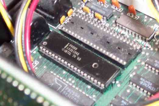
The IBM AT would introduce the 80286. Intel would use a new CPU packaging that would free the address and data buses to dedicated pins thus increasing the pin count to 68 pins. The 80286 was made in several variations including the PLCC - Plastic Leaded Chip Carrier as well as a PGA - Pin Grid Array package. The PLCC is a small flat plastic square with the pins along the sides. This chip presses down into the PLCC socket and is extremely difficult to remove without the proper tools. The PGA package is a small ceramic square with orthogonal rows of pins around the edge of the bottom surface.
80386 132-pin LIF Socket for the PGA Chip 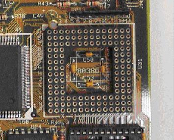
Math Coprocessor, a 68-pin PLCC 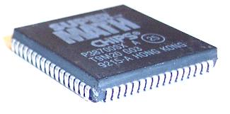
68-pin PLCC Socket (foreground)
132-pin PQFP 386 (background)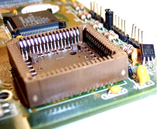
The 80386 was the first full 32-bit microprocessor. Having full 32-bit address and data buses would further increase the CPU pin count for this generation up to 132 pins. The 80386 was made in several variations including the C/PQFP - Ceramic or Plastic Quad Flat Pack a variation of the earlier 68-pin PLCC of the 286 generation as well as a 132-pin PGA package. The C/PQFP is a small flat plastic square with the pins along the sides. This chip presses down into the PQFP socket and is extremely difficult to remove without the proper tools. The PGA package is a small ceramic square with orthogonal rows of pins around the edge of the bottom surface. Because the C/PQFP form factor CPU's were so difficult to remove from their sockets, manufacturers began mounting them on small printed circuit board adapters to the 132-pin PGA form factor for use in many PC's.
80386 132-pin PQFP to PGA Adapter 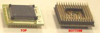
The 80486 was the first microprocessor featuring a clock multiplied core which would need input pins to control it. The 486 also brought internal L1 cache and other advancements which would further push the pin count up to 168/169 pins and then again to 238/239 total pins. The 80486 was made in several variations including the C/PQFP - Ceramic or Plastic Quad Flat Pack, a variation of the earlier 132-pin C/PQFP of the 386 generation as well as PGA packages. The C/PQFP is a small flat plastic square with the pins along the sides. This chip presses down into the PQFP socket and is extremely difficult to remove without the proper tools. The PGA package is a small ceramic square with orthogonal rows of pins around the edge of the bottom surface. Because of the problems with the 386 C/PQFP form factor CPU's most of these were used in laptops and the PGA variations were intended for desktop systems eliminating the need for the C/PQFP to PGA adapters that proliferated in the 386 generation. It was during the 486 generation of processors that Intel introduced the ZIF - Zero Insertion Force socket systems. Prior to these PGA form factor processors had to be pressed firmly down into LIF - Low Insertion Force sockets. However, with the alarming rise in pin count, even LIF sockets were requiing so much force that the processors would easily crack before all of the pins would slide out of the socket holes.
80486 168-pin PGA and motherboard Socket
Socket 4167 is for Weitek Math Coprocessor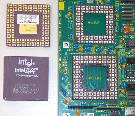
The 486 and beyond processor mounting sockets found on the motherboards featuring the chipsets we have discussed are as follows including the CPU package and generation that they were designed for:
Mount Package Voltage Generation Socket 1 PGA 5V 486's and Pentium Overdrives Socket 2 PGA 5V 486's and Pentium Overdrives Socket 3 PGA 5V, 3.3V 486's and Pentium Overdrives Socket 4 PGA 5V First 5V Pentiums Socket 5 SPGA 3.3V, 3.5V Early low Volt Pentiums Socket 6 PGA 3.3V 486's and Pentium Overdrives Socket 7 SPGA VRM P5x-P54x SS7 SPGA VRM P55x and up Socket 8 Dual pattern SPGA VRM Pentium Pro Slot 1 SEPP/SECC/SECC2 autoVRM PII/III and Celerons Slot 2 SECC autoVRM PII/III Xeons Socket 370 FC-PGA autoVRM PII/III and Celerons Socket 423 FC-PGA autoVRM P4 Socket 478 FC-PGA2 autoVRM P4 Socket M FC-PGA2 autoVRM Pentium M Socket 603 INT3-mPGA autoVRM Xeon Socket J LGA771 autoVRM Xeon Socket T mFC-PGA2 autoVRM P4 Sockets 1, 2, 3, and 6 are 486 processor mounting technologies. Socket 6 was a published Intel design that was never actually manufactured.
237-pin Socket 3 for 80486 processors 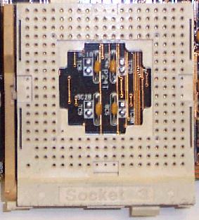
Socket 4 supports the first 5.0V Pentiums which were a very brief generation that also featured PGA chips rather than SPGA. The motherboards that support more than one voltage would have to have a jumper setting.
273-pin Socket 4 for 5V Pentium 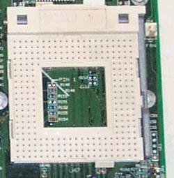
The VRM introduced in Socket 7 allowed manufacturers to continue reducing the voltage requirements of the CPU which led to a boom in CPU speeds. CPUs continue increasing in speed and reducing voltage to the current P4 running on 1.9V. AutoVRM means that the motherboard circuitry and BIOS can be set up as "jumperless" meaning that the motherboard can be wired to autodetect the CPU and set the VRM (Voltage Regulator Module) to the correct voltage(s) for the CPU or the user can enter BIOS and manually set them (not a good idea since this can destroy the CPU rather quickly.) Third party manufacturers would modify Socket 7 to support a 100Mhz front side bus connectivity. AMD processors mounted to these Super Socket 7's would compete with Pentium II's and III's for years and top of the line motherboards supported upgrades of these processors for years making this one of the most successful technologies of this entire series.
320-pin Socket 7 for 3V Pentiums 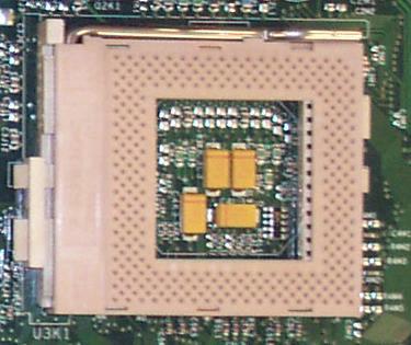
On the subject we need to know what the processor packages are. PGA means Pin Grid Array. The processor is a small silicon wafer embedded in the middle of a flat rectangular gray ceramic shell. One side of this protective shell has evenly spaced rows and columns of pins protruding from it which connect the microprocessor to the motherboard when it is mounted into the socket. SPGA means Staggered Pin Grid Array. The package is similar but the pins do not line up in square rows and columns but are staggered into diagonals instead. This allowed Intel to put more pins than before.
Illustration of Pentium P54 SPGA Form Factor 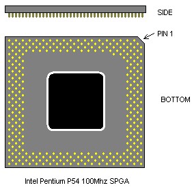
Intel persevered during the 386 with the CQFP - Ceramic Quad Flat Pack, and the PQFP - Plastic Quad Flat Pack packaging, a 132-pin count variation of the PLCC with much finer pins leading to much more easily destroyed sockets and processors. Surplus 386's manufactured with the PLCC form factor were often solder mounted to small circuit boards with standard PGA's on the opposite side to accommodate PGA sockets in which the processor could be easily replaced. Intel would continue this packaging into the 486's. Fortunately OEM’s lost enough money honoring warranties that these easily damaged form factors started to disappear during the early 486 generation.
Illustration of 80486 PGA Form Factor 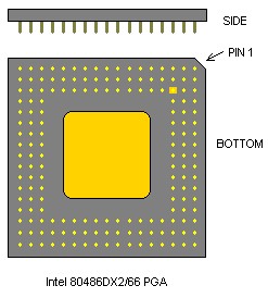
FC-PGA means Flip Chip – Pin Grid Array and is in idea that Intel stole from AMD. It is still basically a large high density SPGA package but the ceramic shell is only half as thick. The top half layer is missing. As such the actual silicon wafer of the CPU is protruding from the top side of the package. The chip takes less material to manufacture, is lighter, and the heat sink/cooling fan assembly when clamped down on the chip is in direct contact with the CPU itself. This reduces the temperature stress on the ceramic package but now a bulky fan must be balanced on a very brittle small silicon chip and damage is very likely with "flip chips."
Illustration of FC-PGA Form Factor 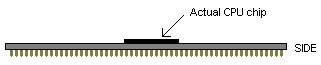
Socket 370 for Intel CPU's in FC-PGA Form Factor 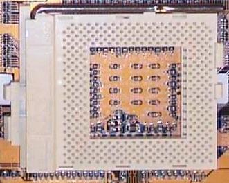
AMD Athlon 650Mhz in FC-PGA Form Factor 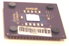
The Intel FC-PGA2 is essentially the same as the FC-PGA except that the overall size of the chip is much smaller and the pin spacing is extremely small. More importantly to the end user/technician is the fact that Intel included what they call the IHS, Integrated Heat Sink. This metal covering of the processor is almost the size of the entire package and provides an excellent platform on which to mount the cooling fan and prevents damage to the chip.
Slot 1 also called SC-242 (Slot Connector) accommodates processors that are mounted on printed circuit boards instead of embedded in flat square ceramic or plastic shells. The SECC (Single Edge Card Connector) features a full plastic shell over both sides of the processor board. SECC packages suffered from cooling problems because of this shell and Intel would modify the design twice.
Pentium II Klamath in SECC Form Factor 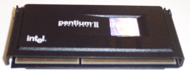
The SEPP - Single Edge Processor Package was introduced in the Celerons and features no plastic shell at all. This arose because the printed circuit board card edge processors of the Pnetium II generation were costing far more than Intel had anticipated. So the SEPP was nothing more than an effort to make the CPU cheaper to manufacture. it would turn out that it was much easier to keep it cool because heat sink/fan assemblies could now come into direct contact with the CPU core itself. This would influence the SECC2 design.
Pentium II Celeron in SEPP Form Factor 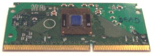
The SECC2 features a plastic shell over the back side of the processor board but not the side that the processor is soldered to. This "Pentium on a half shell" allows a heatsink/fan assembly to clamp to holes in the board at the corners and be in direct contact with the chip itself.
Pentium III Katmai in SECC2 Form Factor 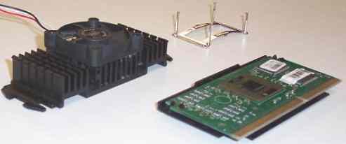
After the brief Socket 423 and the early Pentium 4 "Willamettes" made for it, Intel changed from the very easily damaged FC-PGA form factor to the new mFC-PGA2 form factor introduced on later Willamette Pentium 4's and used throughout the life span of the Socket 478. These processors are far smaller with extremely short and fine pins arranged orthogonally. The ceramic is still only half as thick as the CPU wafer, but the top is shielded by the IHS - Integrated Heat Spreader which physically protects it from damage making this a very easy processor to handle.
Pentium 4 Willamette in mFC-PGA2 Form Factor 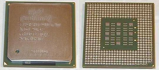
Left to Right: Pentium MMX, AMD FC-PGA, Pentium 4 mFC-PGA2 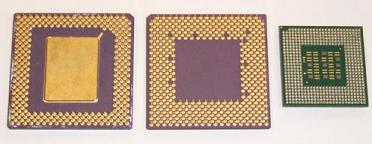
Socket 478 for the mFC-PGA2 CPU 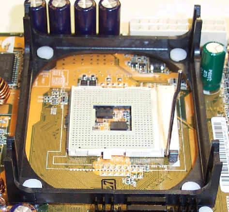
The Socket 478 mounting system would be replaced by the LGA775 mounting system for the standard desktop processor starting with the Prescott core Pentium 4. The processor's form factor is called the FC-LGA and is similar in size and IHS to the mFC-PGA2 predecessors, but the processor has no pins, instead it has a field of 775 tiny copper circles flush with the bottom surface that rest on the 775 pins sticking up from the Socket T mounting system on the motherboard. LGA775, both CPU FC-LGA form factor and Socket T have turned out to be quite user friendly, making FC-LGA processors very easy to install and replace. LGA775 has the necessary pin count to support dual physical core processors which the Socket 478 did not have.
Pentium Extreme Edition in FC-LGA Form Factor 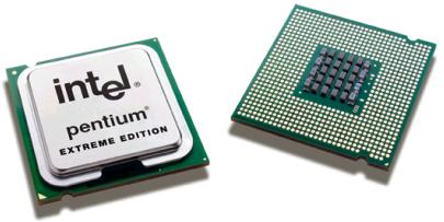
CPU Pins of PGA (left) vs. Lands of LGA (right) 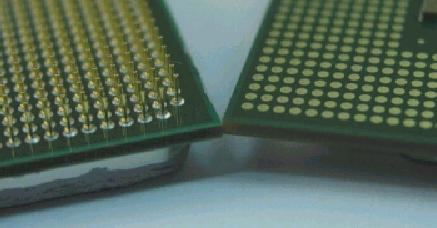
Socket T for the FC-LGA Processors 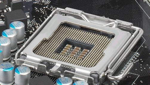
Socket M was influenced by the success of the Intel "Centrino" marketing strategy. One that became so successful that this laptop technology began to appear in desktop systems. However. the BGA - Ball Grid Array, form factors of the mobile processors are made so that those CPU's can be surface soldered directly onto the motherboard. There is almost no way to remove them afterward. Many desktop system owners expect to choose and mount their CPU themselves. This forced Intel to design and manufacture a form factor for the Pentium M for desktop based systems. The Pentium M is not a Family 15 processor and so is not easily compatible with Family 15 motherboards and chipsets. This further pressed Intel to design a unique form factor for the Pentium M which is a modified mFC-PGA2 and the mounting system is a 479-pin socket that looks very similar to Socket 478 called Socket M.
Socket 8 was the first very high pin count mounting system supporting the P6 Dual Independent Bus architecture which separates the front side bus into two complete and independent address buses and data buses, one for the MMU to access RAM and feed the L2 cache and the other for all other transactions. This instantly presented Intel with a huge pin count increase which first appeared in the Pentium Pro as a 387-pin PGA package that would mount into Socket 8.
Pentium Pro in 387-pin PGA Form Factor 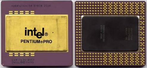
Socket 8 for the 387-pin PGA Form Factor 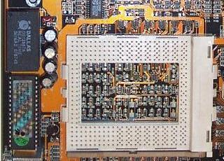
The Family 15 Xeon processors would appear at first in Socket 603/604 variants. Socket 603/604 differ by a single pin that prevents certain combinations of the processors to be mounted onto the incorrect motherboard. Some of these Xeon systems supported single and dual Xeon processors called Xeon DP processors only while others supported 4 or more processors called Xeon MP processors. These are all cores made on the early Family 15 0.18µ and 0.13µ processes.
Dual Socket 603 Xeon Motherboard 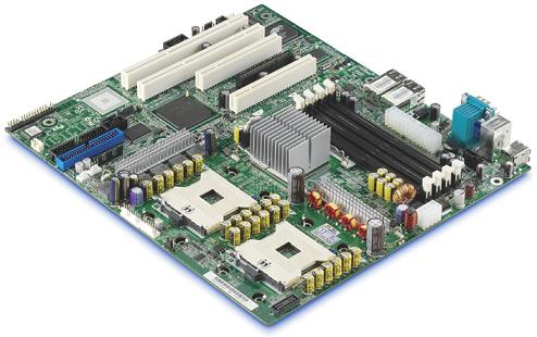
The later Xeon processors made on the 90nm and 65nm processes inherit the lessons learned from the desktop CPU form factors. They are purposely noncompatible but use the same Land Grid Array design in a 771 pin variation. They mount into Socket J.
What was the form factor of the 8088? How was it able to have such a low pin count?
Name the form factors of the 80286. How many pins did these processors have?
Name the form factors of the 80386. How many pins did these processors have?
Name the form factors of the 80486. How many pins did these processors have? List the mounting systems for it.
List the mounting systems for the P5 generation of processors:
You have a 486 motherboard and you have to carefully pry the CPU out of the socket. What type of socket is it?
What was the only Pentium that was packaged PGA, what socket did it use, what chipset generation?
Aside from sockets what was the other method of mounting processors to the motherboard? In what CPU generation was this introduced?
List the processors and their most common manufacturing packages:
You find an old Socket 8 motherboard for sale with processor and RAM. How much L2 cache would you expect to find on the motherboard? What chipset generation will it have? What was the boards probable application?
You have a 166MMX processor and wish to find a motherboard for it. What socket or slot will it have?
What is the major difference between Socket 5 and Socket 7? Explain the implications.
Name the CPU form factors that can be mounted into Slot 1. Name the CPU's found in these form factors.
Name the alternative CPU form factor and mounting system available at the same time as Slot 1. Name the CPU's found in these form factors.
Name the two form factors of the first Pentium 4. Which one was abandoned quickly? Why?
Name the form factor of the latest Pentium 4. What is the motherboard mounting system? Why is it unique from all CPU form factors and mounting systems prior to it?
Although the first Pentium M's did have 478 pins like their contemporary Pentium 4's, what form factor/mounting system did Intel develop for them? Why did they make it different?
Based on the information in this lecture, what is the form factor and mounting system of a Pentium D?
You have an old card edge processor with an Intel logo on it but it does not fit into your Slot 1, what type of processor is it, what is its form factor and mounting system?
What is the form factor and mounting system of 0.18µ Xeon processors?
What is the form factor and mounting system of 65nm Xeon processors?
Explain why the Intel FC-PGA form factor was so unpopular. What form factor replaced it?Is this form factor better? How?
Find out what processor is in your own computer (or a computer here on campus). Based on the processor try to predict the CPU form factor. Carefully and with the owners permission, open the case and verify the form factor of the processor. Many are buried underneath huge heatsink/cooling fan assemblies. If the CPU is a suspected FC-PGA, it is best left alone!
AMD was forced to use their own mounting systems starting with the Intel Pentium II mounted in Slot 1 which they protected by patent. Find out all of the mounting systems of the AMD processors from the direct competitor with Slot 1 until present day and the CPU families designed for them.
Copyright©2000-2007 Brian Robinson ALL RIGHTS RESERVED