PC Repair 3 Lecture #5 - Motherboard Chipsets
Materials: Lecture Only Lecture OnlyObjectives: The major Intel motherboard chipset families,The subfamilies of the chipsets for the 486 generation CPU,The subfamilies of the chipsets for the P5 generation CPU's,The subfamilies of the chipsets for the P6 generation CPU's,The subfamilies of the chipsets for the Family 15 generation CPU's,The terminology of the chipsets,The major south bridges and their features.Competency: The student will become familiar with the various Intel chipset families and know the basic concepts of what the chipset is and what it does. The student will know how to select a motherboard based on the chipset; being able to identify and discuss the features and how they correspond to the performance and design of the computer system. The student will learn the chipset families and be able to identify them. The student will be able to design new systems with a consideration toward matching processor to the motherboard and in the field be able to quickly identify the processor, motherboard, and chipset in order to assess the system at a glance. |
Intel began making full chipsets for the 80486. Intel had been making individual components of the motherboard chipset since the very first PC because the Intel x86 family processors are far from standalone computers in a chip. In order to accomplish anything the chip needs a plethora of support chips which Intel designs side by side with the processor. As time went on, other companies began to manufacture single chips that contained many of these individual chips within a single chip. This reduced manufacturing costs and these companies were able to redesign the chips with their own advances making them faster and more efficient.
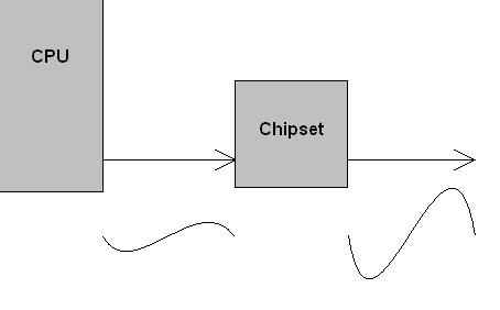
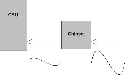
The chipset can then be defined as: the collection of additional circuitry chips that are required in order for the processor to be able to communicate with main memory and any I/O device. Therefore without the chipset the CPU is literally stranded and incapable of communication with any I/O device such as the keyboard for input or the video controller for output, nor can it communicate with RAM meaning that it cannot even execute a single instruction.
Because the CPU relies entirely upon the chipset to "pass along" all of its signals to the rest of the computer system including RAM itself, it stands to reason that superior performance chipsets will directly affect the performance of the CPU which in turn directly affects the performance of the computer as a whole; and this is the situation. The same CPU mounted to two motherboards, one with a poor chipset and the other with a fast and powerful chipset will perform poorly on the first and fast on the other. In fact, fast and powerful chipset based motehrboards can often outperform another poor chipset based system even when the CPU on the low end motherboard is far superior.
The three main functions of the motherboard itself are:
1) Provide a socket or slot for mounting the CPU to the computer.
2) Provide the foundation for mounting the necessary circuitry (the chipset) to interface with the CPU.
3) Provide the foundation for the circuitry (the bus drivers) and the sockets and/or slots for the interface and attachment of optional peripheral components to the system.
The three main functions of the chipset are:
1) Buffering signals to and from the CPU.
2) Latching signals from the CPU, decreasing wavelength to the CPU.
3) Translation of signals to and from the CPU.
The CPU has always been designed around one goal: processing speed. Every other factor is sacrificed in order to gain speed. As a complex circuit chip this includes the current of the signals it generates. When the CPU places an address on the address bus lines, in the case of a P54 Pentium it may well be 3.3V but the amperage of the signals will be measured in microAmps (millionths of an Amp.) Because the signal is so weak, most circuitry including the RAM module chips themselves cannot even detect it at all much less pass the signals through their binary-to-line demultiplexor circuits which will in turn select the correct address cell within the RAM chip. Therefore the chipset must increase the signal current to a level that all of the other chips in the system can use. But these chips are not called "amplifiers" because they must also reduce the current of the signals coming from another component into the CPU. Those components generate enough current on the signal lines such as the data bus wires that they could destroy the internal circuitry of the CPU - remember the CPU was not designed for that, it was designed for speed and speed alone. Because these circuits increase the current on the line going out from the CPU and reduce the current coming into the CPU, this process of "protecting" the CPU from excessive current while bolstering its signals heading outward is called buffering and the chips are called buffers.
-
The second function of the chipset is to prolong the duration of a signal that the CPU places on one of its signal lines. The CPU is running so fast that its signals last such a short period of time that the rest of the circuitry would not have enough time to react to such an event on the wire. Conversely external signals last far too long, through many clock cycles of the CPU when it really only needs these signals to last for one of the front side bus clock cycles. Prolonging signals that would otherwise be lost because they are so short in duration is a process called latching and so many members of the chipset are latches. These latches are also responsible for shortening the duration of the signal coming in to the CPU a process called "edge-triggering." But we will stay with the term "latching" understanding that the process prolongs signals heading out from the CPU and that it shortens the duration of signals coming in to the CPU.

-
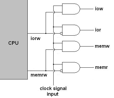
The third function of the chipset is much more complex than simply modifying the electical properties of the signals. The chipset must often translate the meanings of the signals as well. One of the simplest examples is the memrw line and the iorw line of the CPU. These are only valid for specific periods of time during the front side bus clock cycle, otherwise they are invalid. Furthermore, other circuits are not deisgned to use these signals directly anyway. Instead, the chipset will convert these signals into signals that the rest of the circuits will use. The rest of the system would like to see a line that comes on when the CPU is attempting to read from RAM, another that comes on when the CPU is attempting to write to RAM, another that comes on only when the CPU is reading from an I/O address and finally one that comes on when the CPU is writing to an I/O address. Let's also assume that these lines are only valid on the up swing of the front side bus clock signal. Here is the logic:
-
Note that the original output of memrw is "0" = RAM read request only when the clock signal is on the upswing of the waveform .When the clock signal is on the upswing voltage is present which is a valid input for the AND gates. So only when the clock signal is in the correct position would any of the AND gates generate an output. With memrw indicating a read it is "0" so the input to the bottom AND gate is inverted (the little circle in the diagram) With both inputs at "1" now, the memr wire will activate. None of the other AND gates have two "1" inputs and will not activate. Assume the clock is in the upswing (generating voltage = "1") and the iorw line is "1" indicating a "write request to an I/O address" then the top AND gate has its inputs and the iow wire activates, note that the inverter on the second AND gate's iorw input converts the "1" into a "0" and therefore does not satisfy the AND gate's input and the ior wire will not come on.
-
Intel made all of the circuitry components necessary for their CPU's to interface with RAM and other peripheral devices in the original 8086/8088 generation. These were used in the IBM PC motherboard. Here is a list of the important Intel chipset components for the standard IBM AT:
Part Number Component 80286 Microprocessor 80287 FPU, Floating Point (Math) Unit (IRQ 13) 82284 Clock Signal Generator (the Mhz of the chip) 82288 Bus Controller (ISA, 16 bit) 2 x 8254 System Timer Circuit (Programmable, IRQ 0) 2 x 8259 PIC, Programmable Interrupt Controller 2 x 8237 DMA (Direct Memory Access) Controller MC146818 CMOS RAM/RTC (Real Time Clock, IRQ 8) 8042 Keyboard Controller (IRQ 1) After the 486 the FPU has been built into the processor itself. All of the others have modern equivalents in the latest ATX P4 systems. Note that IBM designed and built the IBM AT system and Intel had no chip that did what the MC146818 did. This chip was a very low power consumption (made of CMOS) clock/calendar and featured a built in 64 byte RAM area that could be accessed like a device through I/O ports (70h and 71h). The chip could easily run off of a small battery for months and provide the current date and time to the system through a new BIOS function call. The RAM area could be used to hold hardware settings rather than having to open the machine and change jumpers and/or DIP switches. This is why they incorporated this Motorola chip into the IBM AT motherboard.
During the 486 reign, the chip became so fast and powerful that many third party motherboards were not able to take full advantage of the chip's capabilities. Intel had the manufacturing facilities to make the fastest most complicated chip on earth (the 486) so they also had the facilities to make the fastest and most powerful motherboard chipset chips as well. At first they sold very few chipsets but it is a fair argument that they make the best chipsets since they know the processor like no one else can.
Here are the major Intel chipset generations:
Part Number Generation (82)420xx 486, all (82)430xx P5, all (82)440xx P6, Pentium Pro/PII/PIII/Celerons (82)450xx P6 Servers, Pentium Pro/PII/PIII/Xeons 8xx P6/Family 15 with hub architecture, PIII/P4 all 9xx Family 6/15/CoreTM with hub architecture For example, physically on the motherboard the largest chips are the major members of the chipset. In the lab we found the following part numbers on the two largest chips soldered to the motherboard: “FW82371AB”, and “FW82439TX” We know that the chipset must fall into one of the families listed above. The 82 must be followed by a 42?, 43?, 44?, 45? or 8??. One of them is followed by 439 so this chipset is in the 430xx family meaning that it supports P5’s. As a matter of fact the processor on it is a P200MMX or a P55c. The other chip is what has come to be known as the South Bridge.
A South bridge chip contains all of the slower members of the chipset. Here is a list of other standard devices included in the south bridge: floppy disk drive controller, 2 x UARTs, and 1 x Parallel Port controller. Some early south bridges did not have integral ATA controllers but for the south bridge chips listed they are standard.
Here are the major subfamilies of the 420xx 486 processor chipsets:
Part Number Notes (82)420TX First mass produced Intel motherboard chipset (82)420EX Introduced support for 3.3v processors. Increased front-side bus speed to 50Mhz (82)420ZX Larger amount of RAM supported, PCI 2.1 compliant
Here are the major south bridge chipset members and their features:
Name Part # ATA Controller Integral USB Power Mgmt SIO 82378xx ATA-1 NA SMM PIIX 82371FB ATA-2 NA SMM PIIX3 82371SB ATA-3 1 host/2 ports v1.0 SMM PIIX4 82371AB ATA-4 1 host/2 ports v1.0 SMM PIIX4E 82371EB ATA-4 1 host/2 ports v1.0 SMM/ACPI ICH0 82801AB ATA-4 1 host/2 ports v1.1 SMM/ACPI ICH 82801AA ATA-5 1 host/2 ports v1.1 SMM/ACPI ICH2 82801BA ATA-6 2 hosts/4 ports v1.1 SMM/ACPI ICH3 82801CA ATA-6 2 hosts/4 ports v1.1 SMM/ACPI ICH4 82801DB ATA-6 3 hosts/6 ports v2.0 SMM/ACPI ICH5 82801EB ATA-6/SATA-I 4 hosts/8 ports v2.0 SMM/ACPI ICH5R 82801ER above+RAID 4 hosts/8 ports v2.0 SMM/ACPI The following south bridge chipsets introduce 64-bit PCI 2.3 support and PCI-Express bus support:
| Name | Part # | Integral USB | PCI Support | |
| ICH6 | 82801FB | ATA-6/SATA-I | 4host/8port v2.0 | PCIe 4 x1 chan. |
| ICH6R | 82801FR | above+RAID0 | 4host/8port v2.0 | PCIe 4 x1 chan. |
| ICH6-M | 82801FBM | ATA-6/SATA-I | 4host/8port v2.0 | PCIe 4 x1 chan. |
| ICH7 | 82801GB | ATA-6/SATA-I | 4host/8port v2.0 | PCIe 4 x1 chan. |
| ICH7R | 82801GR | above+RAID0 | 4host/8port v2.0 | PCIe 4 x1 chan. |
| ICH7DH | 82801GDH | ATA-6/SATA-I | 4host/8port v2.0 | PCIe 4 x1 chan. |
| ICH7-M | 82801GBM | above+RAID | 4host/8port v2.0 | PCIe 4 x1 chan. |
| ICH7-M DH | 82801GHM | ATA-6/SATA-I | 4host/8port v2.0 | PCIe 4 x1 chan. |
| ICH7-U | 82801GU | above+RAID | 4host/8port v2.0 | PCIe 4 x1 chan. |
| ICH8 | 82801HB | SATAIIx4port | 5host/10port v2.0 | PCIe 4 x1 + 1 x4 chan. |
| ICH8R | 82801HR | 6port+RAID0/1/5/10 | 5host/10port v2.0 | PCIe 4 x1 + 1 x4 chan. |
| ICH8DH | 82801HH | above+RAID0/1/5/10 | 5host/10port v2.0 | PCIe 4 x1 + 1 x4 chan. |
| ICH8DO | 82801HO | above+RAID0/1/5/10 | 5host/10port v2.0 | PCIe 4 x1 + 1 x4 chan. |
| ICH9 | 82801IB | SATAIIx4port | 6host/12port v2.0 | PCIe 4 x1 + 1 x4 chan. |
| ICH9R | 82801IR | SATAIIx6port+RAID0/1/5/10 | 6host/12port v2.0 | PCIe 4 x1 + 1 x4 chan. |
| ICH9DH | 82801IH | above+RAID0/1/5/10 | 6host/12port v2.0 | PCIe 4 x1 + 1 x4 chan. |
The evolution of the (P)ATA controllers and their ultimate retirement (not appearing in the ICH8 generation), the emergence of SATA, the emergence and proliferation of USB host controllers, and the emergence of ACPI, amidst many other low level technologies too numerous to be listed can be followed through the south bridge family. Later generations bring low voltage VRM adaptations for the lower voltage CPU's and low operating voltage versions specially designed for use in laptops (M designations). Intel mixes and matches north bridges with south bridges as do many other motherboard manufacturers.
SIO means Super I/O and was the first integrated south bridge controller by Intel. It was superceded by the PIIX – PCI to ISA IDE Xcelerator. The main power of this chip was that the ATA controller was "lifted" off of the ISA bus and placed directly on the PCI bus making it 1)PnP, 2)supporting much higher data transfer rates which would influence the evolution of the ATA controllers. The PIIX3 allowed independent device timing on the two IDE channels. Slower devices could be connected on the same controller as faster devices and each would transfer data at its own rate. Previously each ATA channel interface would run at the speed of the slowest device. PIIX4 introduced the ATA-4 controller complete with ATAPI support for booting to CD-ROMs and Iomega Zip Drives as well as running at UDMA mode 2 or 33MB/sec. ICH means I/O Controller Hub. These south bridges belong to the next generation of Intel chipsets made specifically for the P6 and Family 15 generation processors encompassing the PIII and P4 market name processors. The North bridges of Family 15 introduce Rambus memory support, AGP slots and PCI-Express x16 expansion slots.
One of the major limitations of the north bridge chipset is the maximum amount and type of SDRAM supported. The 430TX supports: 2 banks or either FPM/EDO SIMMs or SDRAM DIMMs. On the motherboard we observe 4 SIMM slots, 2 SIMMs complete one memory bank for the Pentium processor, as well as 2 DIMM slots, remembering that 1 DIMM can be a complete memory bank for the Pentium. This is also in complete accordance with the chipset specification. You can attach 4 SIMMs completing 2 banks or 2 DIMMs completing the 2 banks. The 430TX supports a maximum of 256MB of RAM. This means that the largest SIMM possible is 64MB but there were no industry standard 64MB SIMMs manufactured (although proprietary 64MB SIMM's were made they propbably would not function on this generic motherboard) only 32MB. The maximum DIMM possible on this motherboard is 128MB. Buying a pair of 256MB DIMMs would be a waste since the chipset does NOT support this amount of RAM and will either refuse the modules outright, or report and use only half of the DIMMs capacity.
We find that the transition from PCI 2.0 and 2.1 was made during the 430xx generation evolution and that the 430TX supports PCI 2.1. We also see that the chipset does not support ACPI which in fact we do not find in the CMOS Setup Utility, although we do see mention of APM, which is its predecessor. Advanced Power Management is the chipset implementation of SMM interrupt feature in the CPU itself.
You should know that Rambus was introduced in the 8xx series chipsets in the 820 family. This was a long running and prolific family of motherboard chipsets aimed mainly at the late Pentium III generation though a few are backwards compatible for Pentium II processors but certainly only Socket 370 CPUs.
Here are the P5 generation processor chipsets:
| Name | Part# | FSB | RAM Types | Max.RAM | Parity/ECC | S.Bridge |
| Mercury | 430LX | 66Mhz | FPM | 192MB | Parity | SIO |
| Neptune | 430NX | 66Mhz | FPM | 512MB | Parity | SIO |
| Triton | 430FX | 66Mhz | FPM/EDO | 128MB | None | PIIX |
| Mobile Triton | 430MX | 66Mhz | FPM/EDO | 128MB | None | MPIIX |
| Triton II | 430HX | 66Mhz | FPM/EDO | 512MB | Both | PIIX3 |
| Triton III | 430VX | 66Mhz | FPM/EDO/SDRAM | 128MB | None | PIIX3 |
| N/A | 430TX | 66Mhz | FPM/EDO/SDRAM | 256MB | None | PIIX4 |
-
With the 430FX major improvements begin to appear. Parity RAM support is dropped. Parity RAM detects the error and halts the system forcing the user to reboot which is much more trouble than it is worth. The DRAM controller now supports EDO a superior technology to FPM. The shortcoming of the chipset is that it can only support up to 128MB of RAM. The PIIX south bridge is introduced bringing a superior ATA controller and attachment to the PCI bus for the first time.
-
The 430MX is the first chipset specifically designed for laptops. It is a low voltage, low power consumption chipset that generates less heat as well. The MPIIX south bridge is the low voltage, low power consumption version of the PIIX.
-
The Triton II 430HX supports 512MB RAM and either parity or ECC RAM. It will also allow non-parity RAM to be installed. This is a first for chipsets that support parity; allowing the installation of non-parity RAM as an alternative. Previous DRAM controllers that supported parity, would not allow non-parity RAM to be installled. Triton II introduces the PIIX3 soth bridge chipset bringing the third generation ATA controller. Triton II introduces PCI 2.1 as well.
-
The Triton III 430VX supports SDRAM for the first time. This form of RAM was so much faster than the predecessors that it will quickly render edo support deprecated. The 430TX which did not get a code name is a major revision of the Triton III that supports up to 256MB of SDRAM and includes the PIIX4 south bridge equipped with the ATA-4 controller. This would be the first Intel chipset that could boot fomr a CD-ROM.
-
Here are the 440xx chipsets designed for use with the P6 family of processors:
| Part# | CPU | SMP | FSB | RAM Types | Max.RAM | AGP | S.Bridge |
| 440FX | Pentium II | Yes(2) | 66Mhz | EDO/BEDO | 1GB | No | PIIX3 |
| 440LX | Pentium II | Yes(2) | 66Mhz | EDO/SDRAM | 1GB-EDO/512KB-SDRAM | AGP 2x | PIIX4 |
| 440EX | Celeron | No | 66Mhz | EDO/SDRAM | 256MB | AGP 2x | PIIX4E |
| 440BX | PII/III/Celeron | Yes(2) | 66/100 | SDRAM | 1GB | AGP 2x | PIIX4E |
| 440GX | PII/III/Xeon | Yes(2) | 100 | SDRAM | 2GB | AGP 2x | PIIX4E |
| 440ZX | PII/III/Celeron | No | 66/100 | SDRAM | 256MB | AGP 2x | PIIX4E |
-
These chipsets introduce Slot 1 mounting system supporting CPU's with the SC-242 printed circuit board form factor. SDRAM support for the P6 along with much larger maximum RAM support. They also introduce the AGP slot in 1x and 2x speeds.
-
Here are the 450xx Intel chipsets. These were originally designed for servers and high end workstations:
| Part# | CPU | SMP | FSB | RAM Types | Max.RAM | AGP | S.Bridge |
| 450KX | Pentium Pro | Yes(2) | 66Mhz | FPM | 1GB | No | Various |
| 450GX | Pentium Pro | Yes(4) | 66Mhz | FPM | 1GB | No | Various |
| 450NX | PII/III/Xeon | Yes(4) | 100Mhz | FPM/EDO | 8MB | No | PIIX4E |
-
The 450NX chipset was the Pentium II/III generation solution that could support up to 4 processors if they were MPS - Multiprocessor Specification, 1.0 compliant. Those were the Pentium II and III Xeon processors. Despite the fact that this chipset supports up to 8GB of RAM it is unfortunately only EDO modules. Intel felt that the large L2 cache of these processors would compensate and to some degree it did, but SDRAM would have made for much faster much more powerful systems that would still be considered useful ten years later.
-
Around the time of the 450 series of chipsets Intel released the 460GX chipset supporting 1 to 4 Itanium processors in Socket M. Since Itaniums are not x86 processors this information is included for completeness.
-
Here are the 800 series chipsets designed primarily for use with Socket 370 Pentium III processors and later for Family 15 processors:
| Part# | CPU | SMP | FSB | RAM Types | Max.RAM | AGP | S.Bridge |
| 810 | PII/III/Celeron | No | 66/100 | EDO/SDRAM | 512MB | AGP2x1 | ICH/ICH0 |
| 810E | PII/III/Celeron | No | 66/100/133 | SDRAM | 512MB | AGP2x1 | ICH |
| 815 | PII/III/Celeron | No | 66/100/133 | SDRAM | 512MB | AGP4x2 | ICH |
| 815E | PII/III/Celeron | No | 66/100/133 | SDRAM | 512MB | AGP4x2 | ICH2 |
| 815EP | PII/III/Celeron | No | 66/100/133 | SDRAM | 512MB | AGP4x2 | ICH2 |
| 820 | PII/III/Celeron | Yes(2) | 66/100/133 | RDRAM | 1GB | AGP4x3 | ICH |
| 820E | PII/III/Celeron | Yes(2) | 66/100/133 | RDRAM | 1GB | AGP4x3 | ICH2 |
| 840 | PIII/Xeon | Yes(2) | 66/100/133 | RDRAM(dual channel) |
4GB | AGP4x3 | ICH |
| 815P | PIII/Celeron | No | 66/100/133 | SDRAM | 512MB | AGP4x3 | ICH/ICH0 |
| 815GE | PIII/Celeron | No | 66/100/133 | SDRAM | 512MB | AGP2x1 | ICH2 |
| 815G | PIII/Celeron | No | 66/100/133 | SDRAM | 512MB | AGP2x1 | ICH/ICH0 |
1 Integrated video controller built into the motherboard, no expansion slot.
2 Integrated video 2x, expansion slot up to 4x.
3 Expansion slot up to 4x, no integrated video controller.
-
The 800 series of chipsets changed radically the architecture of the motherboard to what Intel refers to as the Intel "Hub" architecture. The chipsets have two separate front side bus interfaces to the CPU, one for I/O and the other for RAM memory. I/O requests are forwarded to the ICH - I/O Controller Hub - south bridge, while the high speed RAM front side bus transactions are forwarded to the MCH - Memory Controller Hub - or north bridge component. The names, like the "810EG" refer to the combination of one particular MCH, with a particular ICH. AGP is a high speed transaction that is routed through the MCH to a modified high speed PCI controller operating at 66Mhz for interface to the video controller either integrated or attached to the AGP slot. These MCH's would be the first to introduce the ill-fated RDRAM - Rambus Dynamic RAM and dual channel versions of it. By the 840 chipset, Intel was already dropping RDRAM and backpeddling quickly to support SDRAM again.
-
The 810 Family of chipsets featured an integrated Intel 3D graphics processor, integrated Intel AC'97 (Audio Codec 1997 specification) compliant sound controller, a 266MB/sec hub interface, and the Intel LPC - Low Pin Count - architecture communication between chipsets is done on multiplexed lines which can act either like the data bus lines or the address bus lines at a very high clock rate.
-
Note: the 810 family support the 133Mhz front side bus speed, but they are running two separate front side buses, furthermore neither of these actually runs at 133Mhz! The MCH is attached at 100Mhz and supports PC100 SDRAM, the ICH is attached to the CPU at 66Mhz, and only the clock signal provided to the CPU is actually running at 133Mhz. With the 815 family, the MCH is attached at 133Mhz and these are the first to allow the installation of PC133 SDRAM modules.
-
The 820 family introduces Rambus or RDRAM. They support AGP 4x expansion slot mounted video controllers but do not offer integrated AGP video controllers in the chipset. RDRAM was not nearly as fast as it claimed but it was as expensive as it claimed and would soon fall into disfavor as it failed to outperform DDR based systems with modules selling for a fraction of the price.
-
The 840 family introduces dual channel Rambus which does have twice the throughput and did for a while outperform DDR based systems. But they were very expensive requiring twin identical modules to be installed, one per channel. The 840 family introduces a separate PCH - PCI controller hub which supports multiple PCI buses for superior performance especially with heavy traffic to the HDD's attached to the high speed bus master capable ATA controllers. These also support 64-bit PCI in either 33Mhz or 66Mhz introducing these variations of the PCI bus slots to the PC industry.
-
Family 15 chipsets span many series and generations. We will start with the 800 series chipsets intended for the Pentium 4 processors:
| Part# | CPU | SMP | FSB | RAM Types | Max.RAM | AGP | S.Bridge |
| 850 | Pentium 4 | No | 4001 | dual channel RDRAM |
2GB | AGP4x2 | ICH2 |
| 850E | Pentium 4 | No | 400/533 | dual channel RDRAM |
2GB | AGP2x1 | ICH |
| 845 | P4/Celeron | No | 400 | PC133-SDRAM DDR200/266 |
3GB-PC133 2GB-DDR |
AGP4x1 | ICH2 |
| 845E | P4/Cel/Cel.D | No | 400/533 | DDR200/266 | 2GB | AGP4x1 | ICH4 |
| 845GL | P4/Cel/Cel.D | No | 400 | PC133-SDRAM DDR200/266 |
2GB | AGP4x2 | ICH4 |
| 845G | P4/Celeron | No | 400/533 | PC133-SDRAM DDR200/266 |
2GB | AGP4x3 | ICH4 |
| 845GE | P4/Celeron | No | 400/533 | DDR266/333 | 2GB | AGP4x3 | ICH4 |
| 845GV | P4/Cel/Cel.D | No | 400/533 | DDR200/266 | 2GB | AGP4x2 | ICH4 |
| 845PE | P4/Celeron | No | 400/533 | DDR266/333 | 2GB | AGP4x1 | ICH4 |
| 865P | P4/Celeron | No | 400/533 | dual channel DDR266/333 |
4GB | AGP8x4 | ICH5/5R |
| 865PE | P4/Celeron | No | 533/800 | dual channel DDR333/400 |
4GB | AGP8x4 | ICH5/5R |
| 865G | P4/Celeron | No | 533/800 | dual channel DDR333/400 |
4GB | AGP8x5 | ICH5/5R |
| 865GV | P4/Celeron | No | 533/800 | dual channel DDR333/400 |
4GB | AGP8x6 | ICH5/5R |
| 875 | P4/Celeron | No | 533/800 | dual channel DDR333/400 |
4GB | AGP8x4 | ICH5/5R |
| 875P | P4/Celeron | No | 533/800 | dual channel DDR333/400 |
4GB(opt.ECC) | AGP8x4 | ICH5/5R |
| 848 | P4/Cel/Cel.D | No | 400/533/800 | DDR266/333/400 | 2GB | AGP8x1 | ICH5x |
1 AGP 1.5V 4x expansion slot, no integrated video controller.
2 No expansion slot, integrated AGP 1.5V 4x video controller.
3 AGP 1.5V 4x expansion slot, with integrated video controller.
4 AGP 1.5V 8x expansion slot, no integrated video controller.
5 AGP 1.5V 8x expansion slot, with integrated video controller.
6 No expansion slot, with integrated AGP 1.5V 8x video controller.
-
Most of the variations within this series of chipsets revolve around the AGP architecture. Intel either includes an 200Mhz Intel Extreme Graphics series processor (AGP 4x or an AGP 8x Intel Extreme Graphics 2 processor) or a low voltage AGP 4x (or 8x) slot or both. The 845 family drops Rambus in favor of AMD's RAM technology: DDR.
-
With the growing popularity of DDR the 845 series would carry Intel for several years. ICH5 series south bridges bring PCI 2.3 and ATA RAID capabilities to the desktop PC industry (not just high end servers and workstations.)
-
The 900 series was introduced in 2004 and would continue service until the present (c.2007) with the Family 15 "Pentium 4" line of processors.
| Part# | CPU | SMP | FSB | RAM Types | Max.RAM | AGP | S.Bridge |
| 915P | P4/Celeron | No | 533/800 | dual channel DDR333/400,DDR2 |
4GB | PCIe x16 | ICH6x |
| 915G | P4/Celeron | No | 533/800 | dual channel DDR333/400,DDR2 |
4GB | PCIe x161 | ICH6x |
| 915GV | P4/Celeron | No | 533/800 | dual channel DDR333/400,DDR2 |
4GB | AGP 8x2 | ICH6x |
| 915GL | P4/Celeron | No | 533 | dual channel DDR333/400 |
4GB | AGP 8x2 | ICH6x |
| 925XE | P4(90nm) | No | 800/1066 | dual channel DDR2-400/533 |
4GB | PCIe x161 | ICH6x |
1 PCI-Express x16 expansion slot, no integrated video controller. 2 No PCI-Express x16 expansion slot, with AGP 8x integrated video controller.
-
Intel began producing the Pentium D, true dual core Family 15 processors that were literally two Pentium 4's in a single package. These chipsets support these CPU's:
| Part# | CPU | SMP | FSB | RAM Types | Max.RAM | AGP | S.Bridge |
| 925X | P4/P4EE | No | 800 | dual channel DDR2-400/533 |
4GB | PCIe x161 | ICH6x |
| 945PL | P4/D/Cel | No | 533/800 | DDR2-400/533 | 2GB | PCIe x161 | ICH7x |
| 945P | P4/D/Cel | No | 533/800/1066 | dual channel DDR2-400/533/667 |
4GB | PCIe x161 | ICH7x |
| 945GZ | P4/D/Cel | No | 533/800 | DDR2-400/533 | 2GB | Intel 950 GPU | ICH7x |
| 945G | P4/D/Cel | No | 533/800/1066 | dual chan. DDR2 400/533/667 |
4GB | Integrated 950 GPU | ICH7x |
| 955X | P4/D/P4EE/XE1 | No | 800/1066 | dual channel DDR2-533/667 |
8GB | PCIe x161 | ICH6x |
-
These chipsets form part of the Intel brand name "Centrino" which consists of a system equipped with a Pentium M processor, one of these chipsets and the Intel/PRO wireless LAN series of adapters (usually integrated into the motherboard.)
| Part# | CPU | FSB | RAM Types | Max.RAM | Vid | S.Bridge |
| 855 | Pentium M | 533/800/1066 | DDR2 | 4GB(opt.ECC) | PCIe x161 | ICH6x |
| 915GM | Pentium M | 533/800 | DDR2 | 4GB(opt.ECC) | Integrated | ICH6x |
| 915PM | Pentium M | 533/667/800 | DDR2 | 8GB(opt.ECC) | PCIe x16 slot | ICH6x |
| 915GMS | Pentium M | 533/667 800/1066 |
DDR2 | 8GB(opt.ECC) | Integrated | ICH6x |
| 945GT | Pentium M Core Duo |
533/667 | dual ch. DDR2 400/533/667 |
4GB | Intel 3.5 GPU | ICH7-M |
| 965PL | Core Solo |
533/667 | dual ch. DDR2 533/667 |
4GB | PCIe x16 | ICH8-M |
| 965GM | Core Solo |
533/667 | dual ch. DDR2 533/667 |
4GB | Intel X3100 GPU | ICH8-M |
-
915GMS is an ultra low voltage chipset and runs only ultra low voltage CPU's intended primarily for laptops. This was done to create a ditinguished chipset for laptops because the power of the Pentium M and the 915M series chipsets in the "Centrino" brand name was causing manufacturers to build desktop "Centrino" systems. Laptops would need a "truly designed for portable systems" technology with this architecture.
-
When motherboards based on these chipsets are equipped with a Pentium Core Duo (a true dual core Pentium M processor) then they are called "Centrino Duo" When they are equipped with a Celeron M processor some manufacturers call these systems "Celeron Cetrino" but according to Intel, Celeron Centrino does not exist and this is an erroneous claim.
-
Chipsets for the current Intel CoreTM Architecture family of CPU's marketed as Core Solo, Core 2 Duo, Core 2 Extreme, and Core 2 Quad.
| Part# | CPU | SMP | FSB | RAM Types | Max.RAM | AGP | S.Bridge |
| 975X | P4/D/P4EE- XE/C2D/C2E1 |
Yes(2) | 533/667- 800/1066 |
dual channel DDR2-533/667 |
8GB | PCIe x161 | ICH7x |
| 946PL | P4/D/P4EE- XE/C2D1 |
No | 533/800 | dual channel DDR2-533/667 |
4GB | PCIe x162 | ICH7x |
| 946GZ | P4/D/P4EE- XE/C2D1 |
No | 533/800 | dual channel DDR2-533/667 |
4GB | Intel 3000 GPU | ICH7x |
| Q963 | P4/D/C2D1 | No | 533/800/1066 | dual channel DDR2-667 |
8GB | Intel 3000 GPU2 | ICH8x |
| G965 | P4/D/C2D1 | No | 533/800/1066 | dual channel DDR2-667 |
8GB | Intel X3000 GPU2 | ICH8x |
| P965 | P4/D/C2D1 | No | 533/800/1066 | dual channel DDR2-533/667 |
8GB | PCIe x163 | ICH8x |
| Q965 | P4/D/C2D1 | No | 533/800/1066 | dual channel DDR2-533/667 |
8GB | Intel 3000 GPU2 | ICH8x |
2 Provides PCI-Express x16 slot plus integrated Intel 3000/X3000 GPU
3 Provides PCI-Express x16 slot with no integrated GPU
-
These chipsets are intended for high0end workstation and server platforms. Intel chose to omit multiple CPU capability of their standard chipset families starting with the Family 15 processors. Instead such systems would have to be based on an entirely different (and obviously more expensive) chipset product.
| Part# | CPU | SMP | FSB | RAM Types | Max.RAM | S.Bridge |
| E7210 | Pentium 4 | No | 533/800 | DDR266/333/400 | 4GB(ECC) | 6300ESB |
| E7221 | P4 w/HT | No | 533/800 | d.ch.DDR-333/400 d.ch.DDR2-400/533 |
4GB(ECC) | ICH6R |
| E7230 | P4/D w/HT | No | 533/800/1066 | dual channel DDR2-400/533/667 |
8GB(ECC) | ICH7x |
| E7320 | 64-bit Xeon w/2MB Xeon w/1MB @800Mhz |
Yes(2) | 800 | d.ch.DDR-266/333 d.ch.DDR2-400 |
16GB(ECC) | ICH5R 6300ESB |
| E7520 | 64-bit Xeon w/2MB Xeon w/1MB @800Mhz |
Yes(2) | 800 | d.ch.DDR-266/333 d.ch.DDR2-400 |
16GB(ECC) | ICH5R 6300ESB |
| E7501 | Xeon w/512KB @533Mhz | Yes(2) | 400/533 | d.ch.DDR-200/266 | 16GB(ECC) | ICH3S |
| E7505 | Xeon w/512KB L2 | Yes(2) | 400/533 | DDR266 ECC Registered 2.5V |
16GB | ICH4 |
| E7525 | 64-bit Xeon w/2MB Xeon w/1MB @800Mhz |
Yes(2) | 800 | d.ch. DDR2-400 d.ch. DDR-333 |
16GB | ICH5x |
| E7500 | Xeon w/512KB | Yes(2) | 400 | d.ch. DDR-200/266 Registered 2.5V |
16GB(ECC) | ICH3S |
| E8500 | 64-bit Xeon MP | Yes(4) | 667 | d.ch. DDR-200/266 d.ch. DDR2-400 |
128GB (Reg.ECC) |
ICH5 |
| 3000 | Pentium D | No | 533/800/1066 | d.ch. DDR2-533/667 | 8GB(ECC) | ICH7x |
| 3010 | Pentium D | No | 533/800/1066 | d.ch. DDR2-533/667 | 8GB(ECC) | ICH7x |
| 5000X | Dual Core Xeon 5000 Series |
Yes(2) | 1066/1333 | DDR2-533/667 Fully Buffered |
64GB | ICH5x |
NOTE: "d.ch." means Dual Channel.
-
While many of the workstation and server series of chipsets use the same south bridges as the mainstream counterparts, there are some south bridges intended specifically for the workstation and server series north bridges. These mainly include PCI-X (64-bit @ 100Mhz PCI not to be confused with PCI-Express).
| Name | Part # | Integral USB | Features | |
| ICH3S | 82801CA | ATA-6 | 3 hosts/6 ports v1.1 | SMM/ACPI |
| 6300ESB | ? | ATA-6/SATA-I | 3 hosts/6 ports v2.0 | PCI-X(64/66) |
| 631xESB and 632xESB | ATA-6/SATA-II | 5hostX8port v2.0 | PCIe 4 x1 + 2 x4 + 1 x8 + PCI-X(32/64-66/100/133) |
|
List and briefly describe the basic functions of the motherboard:
List and briefly describe the basic functions of the chipset:
List the standard IBM AT motherboard chipset components and part numbers:
Which of the chips above is not made by Intel and who does make it?
Aside from the devices listed above, what other three devices are found in south bridges?
Aside from the devices listed above, what two other devices have been incorporated into the modern south bridges?
What is the main difference between north and south bridges?
List the motherboard chipset generation part numbers and the processor generation(s) they support:
List the south bridge chipset part numbers, common names, integrated ATA controllers, integrated USB controllers, power management support for P5 chipsets:
List the south bridge chipset part numbers, common names, integrated ATA controllers, integrated USB controllers, power management support, and PCI support for P6 chipsets:
List the south bridge chipset part numbers, common names, integrated ATA controllers, integrated USB controllers, and PCI/PCIe support for the 800/900 series chipsets:
What south bridge chipset (name and part number) introduced EIDE?
What south bridge chipset (name and part number) introduced USB 1.0?
What south bridge chipset (name and part number) introduced USB 1.1?
What south bridge chipset (name and part number) introduced USB 2.0?
What south bridge chipset (name and part number) introduced ACPI?
What south bridge chipset (name and part number) introduced ATA-4?
What south bridge chipset (name and part number) introduced ATA-5?
What south bridge chipset (name and part number) introduced ATA-6?
What south bridge chipset (name and part number) introduced ATA 133MB/sec support?
What south bridge chipset (name and part number) introduced SATA-I?
What south bridge chipset (name and part number) introduced SATA-II?
What south bridge chipset (name and part number) introduced PCI-Express x1 slots?
What south bridge chipset (name and part number) introduced PCI-Express x4 slots?
What south bridge chipset (name and part number) introduced PCI-Express x8 slots?
What south bridge chipset (name and part number) introduced PCI-Express x16 slots?
What south bridge chipset (name and part number) introduced integral RAID0?
What south bridge chipset (name and part number) introduced integral RAID1?
What south bridge chipset (name and part number) introduced 4 USB hosts and support for up to 8 integrated USB ports?
Based only on the basic information provided in this lecture module what is the difference between the ICH3S and the rest of the ICH3 family?
Based only on the basic information provided in this lecture module what is the difference between the workstation/server 6300 series south bridges and the main stream south bridges?
What was the first mass produced Intel chipset and what CPU did it support?
Name the south bridges that follow the major transitions of the ATA controller from its humble beginnings to UDMA. These were featured in which major chipset generation?
Name the south bridges that accompany the chipset generation that introduced Rambus. Which generation is this?
What 486 chipset would you prefer to use with a SCSI PCI host controller? Why?
You are thinking of buying a used Pentium II motherboard, what is the highest version USB host controller you would be able to find in it?
You have a 166MMX processor and wish to find a motherboard for it. What chipset generation will it have? What is the fastest ATA controller would you expect to find?
Did they make any 440xx generation motherboards that featured ACPI? If so what south bridge would it have? What ATA controller would it have? What USB controller?
You find a motherboard that takes RIMMs (Rambus Inline Memory Modules). Will it have USB controllers? What is the slowest ATA controller in could have? Will it feature ACPI?
What south bridge chipset (name and part number) would have been the first one that would allow the system to boot from a CD-ROM? First to support ATA100? First to support 480Mbps USB devices?
What north bridge chipset (name and part number) introduced support for EDO RAM? How much RAM could it support?
What north bridge chipset (name and part number) introduced support for SDRAM? How much RAM could it support?
What north bridge chipset introduced support for more than one CPU? How much and what type of RAM could it support?
What north bridge chipset introduced support for more than one CPU and SDRAM? How much RAM could it support?
What north bridge chipset introduced support for a 100Mhz FrontSide Bus? How much RAM could it support?
What north bridge chipset introduced support for a 100Mhz FrontSide Bus and up to 2GB of RAM? How many and what types of CPU could it support?
Based on the CPU supported, what north bridge chipset introduced support for PAE (more than 4GB RAM)? How many and what types of CPU could it support?
What north bridge chipset introduced support for 133Mhz FSB? How much and what type of RAM could it support?
What north bridge chipset introduced support for RDRAM (Rambus)? How much RAM could it support? What CPU was it designed for?
What north bridge chipset introduced support for dual channel RDRAM (Rambus)? How much RAM could it support? What CPU was it designed for?
What north bridge chipset introduced support for DDR? How much RAM could it support? What CPU was it designed for?
What north bridge chipset introduced support for dual channel DDR? How much RAM could it support? What CPU was it designed for?
What north bridge chipset introduced support for DDR2? How much RAM could it support? What CPU was it designed for?
What north bridge chipset introduced support for DDR2-533? How much RAM could it support? What CPU was it designed for?
What north bridge chipset introduced support for DDR2-667? How much RAM could it support? What CPU was it designed for?
What north bridge chipset introduced support for 400Mhz FSB? What is the true clock speed of this FSB? Why is it called 400Mhz? How much RAM could it support? What CPU was it designed for?
What north bridge chipset introduced support for 533Mhz FSB? What is the true clock speed of this FSB? Why is it called 533Mhz? How much RAM could it support? What CPU was it designed for?
What north bridge chipset introduced support for 800Mhz FSB? What is the true clock speed of this FSB? Why is it called 800Mhz? How much RAM could it support? What CPU was it designed for?
What north bridge chipset introduced support for 1066Mhz FSB? What is the true clock speed of this FSB? Why is it called 1066Mhz? How much RAM could it support? What CPU was it designed for?
What north bridge chipset introduced support for 1333Mhz FSB? What is the true clock speed of this FSB? Why is it called 1333Mhz? How much RAM could it support? What CPU was it designed for?
What north bridge chipset introduced support for Registered 2.5V RAM modules? How much RAM could it support? What CPU was it designed for?
What north bridge chipset introduced support for Fully Buffered RAM modules (DDR3)? How much RAM could it support? What CPU was it designed for?
What north bridge chipset introduced support for dual core processors? How much RAM could it support? What CPU was it designed for?
What north bridge chipset introduced support for AGP? How much RAM could it support? What CPU was it designed for?
What north bridge chipset introduced support for AGP 4x? How much RAM could it support? What CPU was it designed for?
What north bridge chipset introduced support for AGP 8x? How much RAM could it support? What CPU was it designed for?
What north bridge chipset introduced support for PCI-Express x16? How much RAM could it support? What CPU was it designed for?
What north bridge chipset introduced support for 16GB RAM? What type(s) of RAM could it support? What CPU was it designed for?
What north bridge chipset supports the most RAM? What type(s) of RAM could it support? What CPU was it designed for?
List the north bridge chipsets that are part of the various Intel Centrino technologies. List how much RAM each supports. List the supported CPU's.
Find out what chipset is in your own computer (or a motherboard you find for sale at a store). Based on the chipset determine: The CPU(s) supported, the (S)ATA controller and its maximum transfer rate, the version of USB supported, whether ACPI is supported, type(s) of PCI and PCI-Express supported, type of video controller supported (AGP or PCIe x16,) whether video controller is integrated, and what type of RAM and the amount that is supported. Bear in mind that the system may not have an Intel chipset, in that case you will have to look up the chipset specifications on the manufacturer's website. Once you have made these predictions open the case and confirm the type and number of expansion slots, presence or absence of integrated video, type and number of RAM slots available. (Some motherboard manufacturers "cut down" the motherboard and do not provide all expansion and/or RAM slots that the chipset could support.) Enter the BIOS and confirm the hard drive's transfer rate (mode), and whether the system supports ACPI.
Copyright©2000-2007 Brian Robinson ALL RIGHTS RESERVED